Thin metal layers-having ceramic green sheet and method for producing ceramic capacitor
a technology of ceramic capacitors and green sheets, which is applied in the direction of manufacturing tools, fixed capacitor details, fixed capacitors, etc., can solve the problems of non-uniform contraction to induce strain separation between the internal electrodes, and contraction over the whole ceramic green sheet, etc., to achieve uniform contraction, good adhesion, good wettability
- Summary
- Abstract
- Description
- Claims
- Application Information
AI Technical Summary
Benefits of technology
Problems solved by technology
Method used
Image
Examples
example 1
[0126] A base film 2 made of a polyethylene terephthalate film a surface of which was subjected to a silicone mold releasing treatment was prepared (see FIG. 5(a)), and a first thin metal layer 4 made of a thin nickel film was formed on the whole surface of the base film 2 to a thickness of 0.08 μm by use of a vacuum deposition apparatus (see FIG. 5(b)).
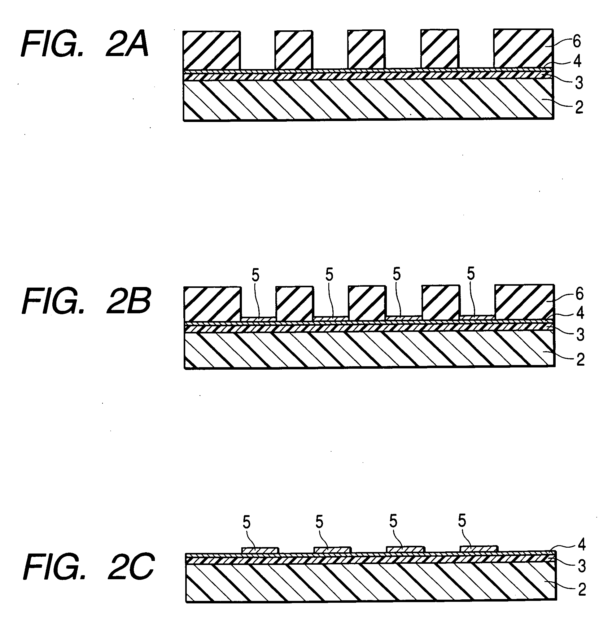
[0127] Then, a plating resist 6 made of a dry film resist was press-bonded onto the whole surface of the first thin metal layer 4 with heat, and thereafter, the plating resist 6 was exposed to light and developed, thereby forming a pattern reverse to a wiring circuit pattern (see FIG. 2(a), however, in this embodiment, the resin layer 3 is omitted).
[0128] Then, a second thin metal layer 5 was formed on the first thin metal layer 4 to a thickness of 0.2 μm by electrolytic nickel plating using the first thin metal layer 4 as an electrode (see FIG. 2(b), however, in this embodiment, the resin layer 3 is omitted). Thereafter, the plati...
example 2
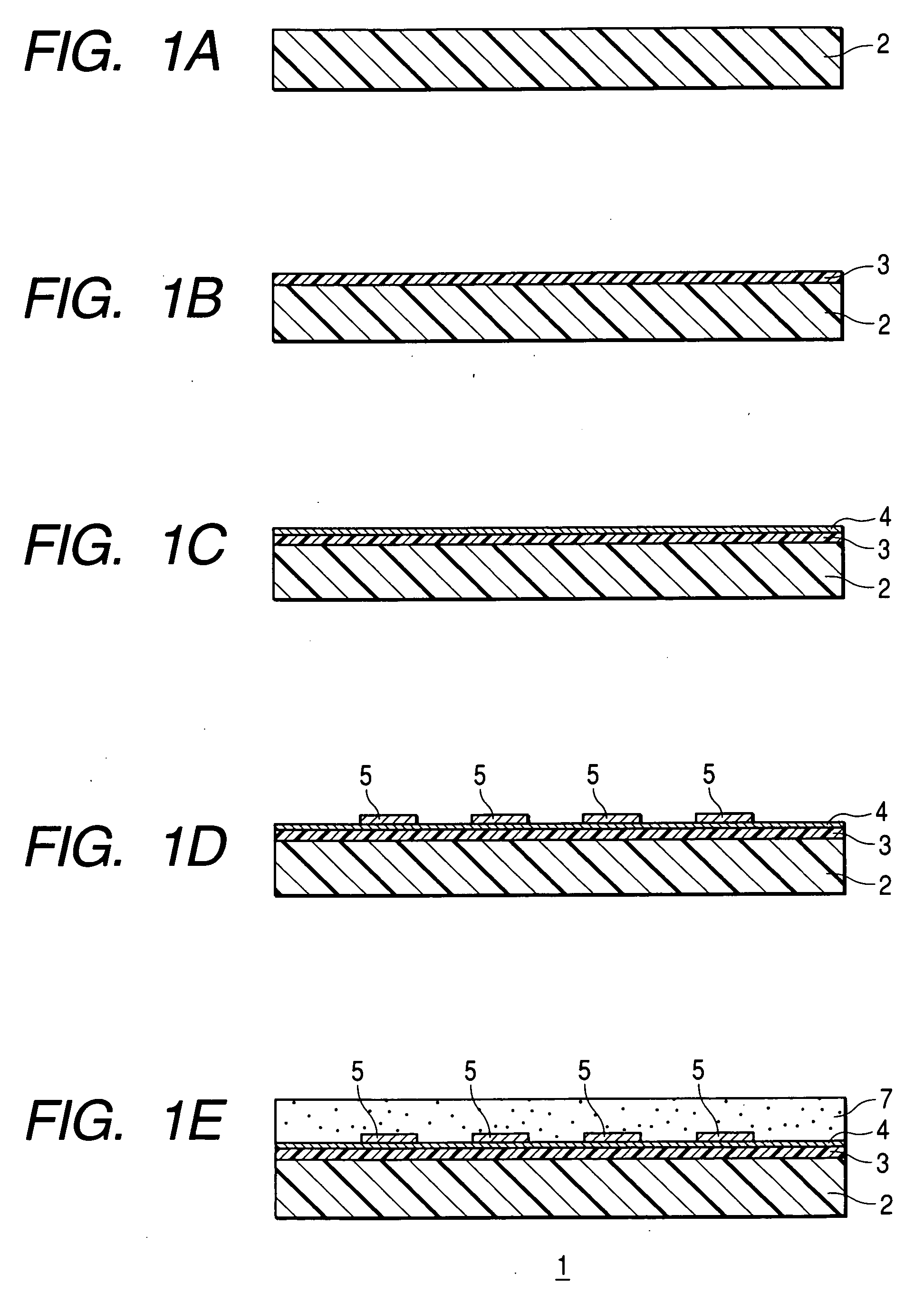
[0140] A base film 2 made of a polyethylene terephthalate film a surface of which was subjected to a silicone mold releasing treatment was prepared (see FIG. 1(a)), and a solution of ethyl cellulose, the same material as the binder of the ceramic powder-dispersed layer 7, in a mixed solvent of toluene and monomethyl glycol was applied thereon by spin coating to a thickness of 0.5 μm as a resin layer 3 (see FIG. 1(b)).
[0141] Then, a first thin metal layer 4 made of a thin nickel film was formed on the whole surface of the resin layer 3 to a thickness of 0.08 μm by use of a vacuum deposition apparatus (see FIG. 1(c)).
[0142] Then, a plating resist 6 made of a dry film resist was press-bonded onto the whole surface of the first thin metal layer 4 with heat, and thereafter, the plating resist 6 was exposed to light and developed, thereby forming a pattern reverse to a wiring circuit pattern (see FIG. 2(a)).
[0143] Then, a second thin metal layer 5 was formed on the first thin metal lay...
PUM
| Property | Measurement | Unit |
|---|---|---|
| thickness | aaaaa | aaaaa |
| thickness | aaaaa | aaaaa |
| thickness | aaaaa | aaaaa |
Abstract
Description
Claims
Application Information


