Chamber stability monitoring using an integrated metrology tool

a metrology tool and chamber stability technology, applied in the direction of semiconductor/solid-state device testing/measurement, individual semiconductor device testing, instruments, etc., can solve the problems of difficult to etch features with high aspect ratio using conventional substrate processing techniques, difficult for reactants to penetrate deep into trenches, and difficult for reaction by-products to be transported from inside the trenches back to the substrate surface, etc., to achieve the effect of shortening the process development cycle tim

Inactive Publication Date: 2005-02-10
APPLIED MATERIALS INC
View PDF12 Cites 21 Cited by
  • Summary
  • Abstract
  • Description
  • Claims
  • Application Information

AI Technical Summary

Benefits of technology

[0009] The invention relates to a method and apparatus for monitoring the stability of a process chamber by measuring characteristics of material layers on a substrate with an integrated metrology tool. The invention trends the calculated process rate, which could include etch rate and deposition rate, of each wafer processed by the process chamber by measuring the film thickness on the substrate before and after substrate processing, and by recording the total process time to detect any process drift to prevent substrate mis-processing. The invention also utilizes the trended process rate and pre-process thickness measurement of the incoming wafer in adjusting the process recipe in real time to tighten the process control. Lastly, the invention also shortens process development cycle time by utilizing real time process information.

Problems solved by technology

It is difficult to etch features having high aspect ratio using conventional substrate processing techniques, especially when the features also have small opening sizes.
It is difficult for reactants to penetrate deep into the trench through small openings and difficult for reaction by-products to be transported from inside the trench back out to the substrate surface through the same small openings.

Method used


Image

  • Chamber stability monitoring using an integrated metrology tool
  • Chamber stability monitoring using an integrated metrology tool
  • Chamber stability monitoring using an integrated metrology tool

Examples


Embodiment Construction

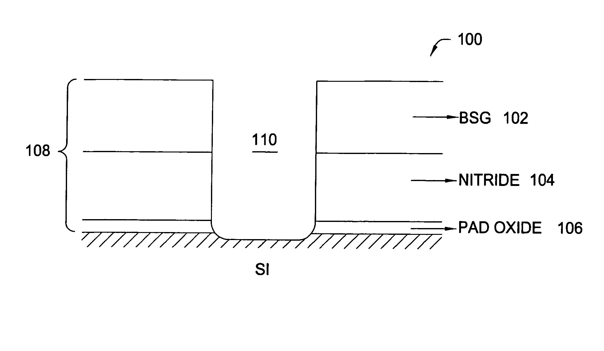
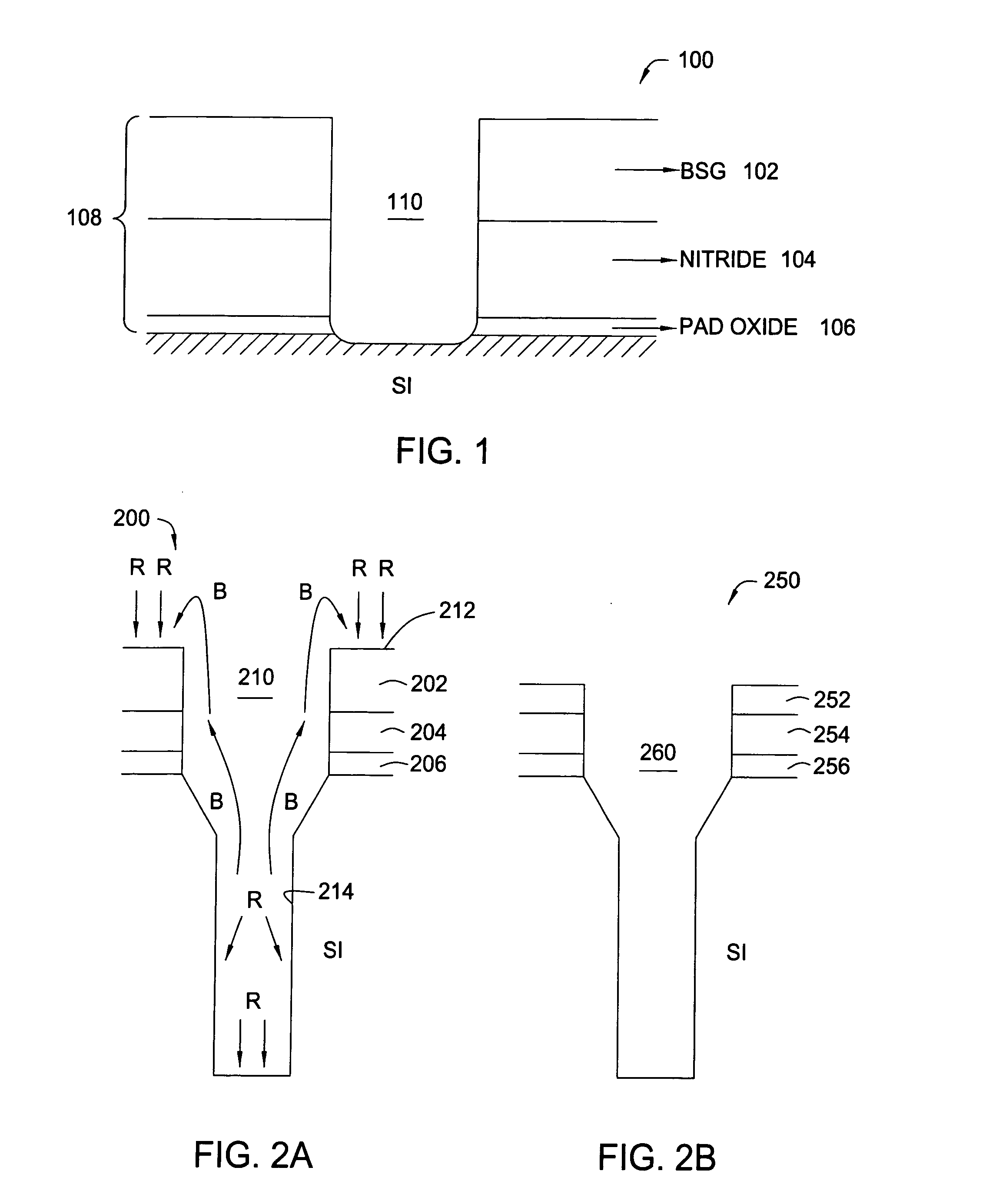
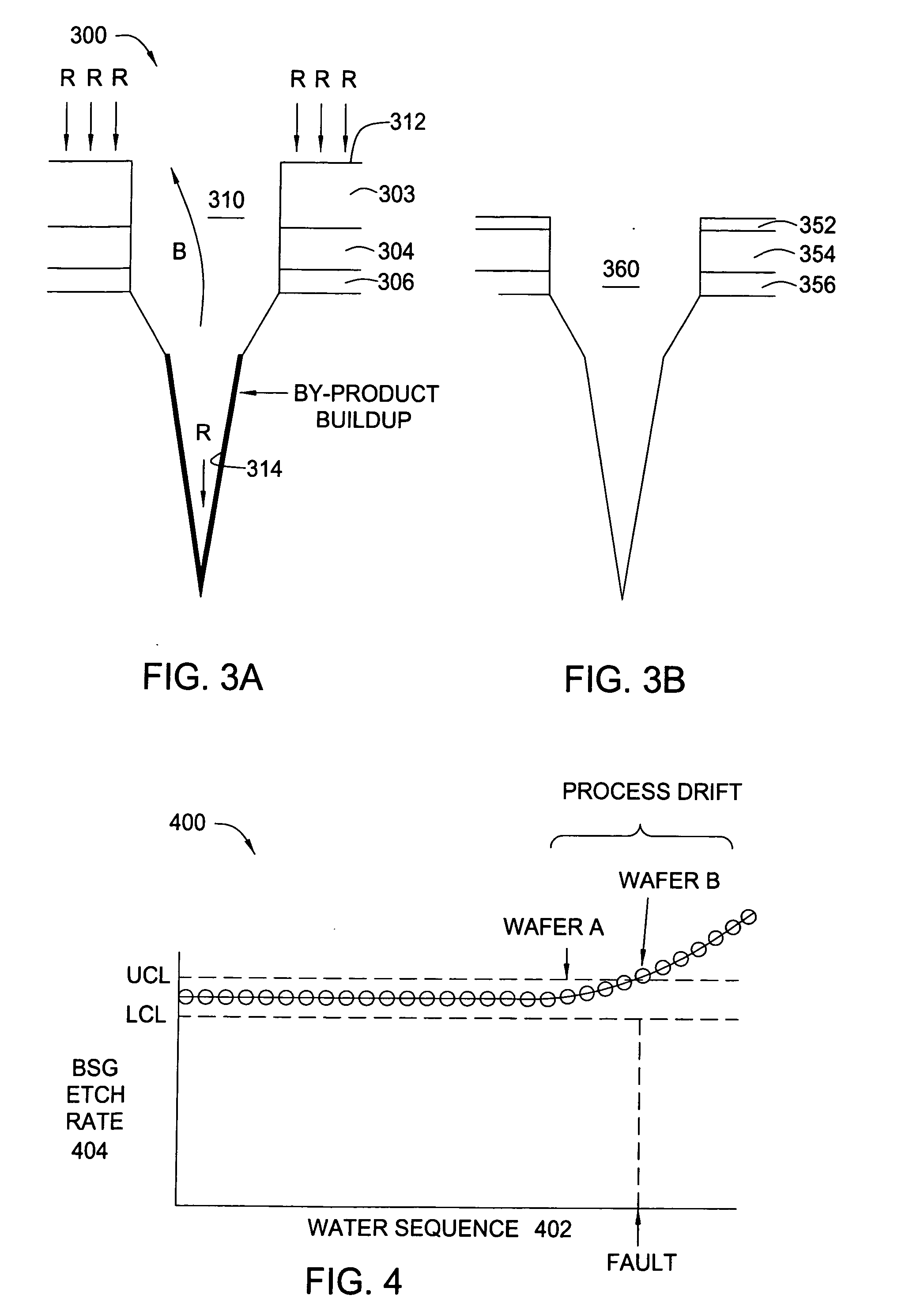
[0023] Semiconductor device fabrication requires feature patterning. When the device being fabricated is a DRAM, one step in the device fabrication process is silicon deep trench etching to form trench capacitors. The present invention is a method and apparatus that finds use in device fabrication and is especially useful in deep trench etching.

[0024] More specifically, the invention measures the thickness of a material layer on a substrate using an integrated metrology tool that is coupled to a substrate processing chamber (e.g., a deep trench etch system). The measurement data are utilized and tracked by the substrate-processing chamber to adjust a process recipe in real time, and to detect process drift. As such, the real time adjustment of the process recipe facilitates accurate processing of the substrate. The real time process information also assists in shortening the process development cycle.

[0025] For convenience, the present invention is described herein primarily with ...


PUM


Abstract

A method and apparatus for monitoring the stability of a substrate processing chamber and for adjusting the process recipe. Thickness and CD measurement data are collected before wafer processing and after wafer processing by an integrated or an in-situ metrology tool to monitor process chamber stability and to adjust the process recipe. The real time chamber stability monitoring enabled by the integrated metrology tool reduces the risk and cost of wafer mis-processing. The real time process recipe adjustment allows tightening of the process recipe. Process development cycle can also be reduced by the method and apparatus.

Description

BACKGROUND OF THE INVENTION [0001] 1. Field of the Invention [0002] The present invention relates to semiconductor substrate processing systems. More particularly, the present invention relates to techniques for monitoring the chamber stability and, in response, adjusting a process recipe to optimize substrate processing. [0003] 2. Description of the Related Art [0004] Current demands for high density and performance associated with ultra large scale integration require sub-micron features, increased transistor and circuit speeds and improved reliability. Such demands require formation of device features with high precision and uniformity, which in turn necessitates careful process monitoring, including frequent and detailed inspections of the devices before the semiconductor wafers are diced into individual circuit chips. [0005] Early detection of chamber fault or process drift is highly desirable, since it can prevent wafer mis-processing, which in turn reduces wafer scrapping, wa...

Claims


Application Information

Patent Timeline
Patent Type & Authority Applications(United States)
IPC IPC(8): H01L21/3065H01L21/308H01L21/66
CPCH01L21/3065H01L22/20H01L21/3081H01L22/00
Inventor MUI, DAVID S.L.LIU, WEISASANO, HIROKI
Owner APPLIED MATERIALS INC
Why Eureka
Try Eureka