[0017] Aspects of the invention are found in a system for thinning wafers. The system comprises a type of dry plasma etcher that utilizes a magnetic mirror technique (i.e., a “magnetic mirror plasma”) and may have one or more additional etchers. The additional etchers may comprise dry etchers, wet etchers, or a combination of dry and / or wet etchers. The potential additional dry etchers may comprise, for example, one or more ion-miller, plasma, or reactive ion etchers, among others. The dry etchers may operate at pressures at, below, or above atmospheric pressure. Further, each plasma etcher may use various means of forming a plasma, including, for example, microwave, radio frequency, inductive, and arc methods, among others. Similarly, the wet etcher may utilize various chemicals. These chemicals may be, for example, customized for the material being etched. Moreover, the various chemicals or chemical combinations may be selected for their degree of specificity and isotropic nature.
[0018] An aspect of the invention may be found in a magnetic mirror plasma. A magnetic mirror plasma uses a unique method to confine a plasma using a magnetic mirror field and an orthogonally rotating electric field. The vector cross product of these orthogonal fields provides the capability for control of ion momentum parallel to the magnetic field lines while leveraging the ion's angular momentum to optimize dissociation of complex process gases into neutral reactive species. Further, to ensure the proper flow control and barrier to neutral partial diffusion, a chamber constructed of non-ferrous material is used to house the substrate being processed. Lastly, the ions confined with the magnetic mirror plasma are created remote to the confinement by an ion source of many possible types.
[0019] Magnetic mirror fields have historically been used in high energy physics experiments and efforts such as fusion energy. For this reason most prior art may be found in patents granted to the U.S. Department of Energy. Magnetic mirror fields have typically not been used in the most common plasma process application of semiconductor thin film etch and deposition due to substrate damage. In the case of high energy physics and fusion energy experimentation, substrate processing is not the objective. Rather, plasma confinement is the primary objective of these high energy experiments and as such orthogonal electric fields have been considered to be a detriment.
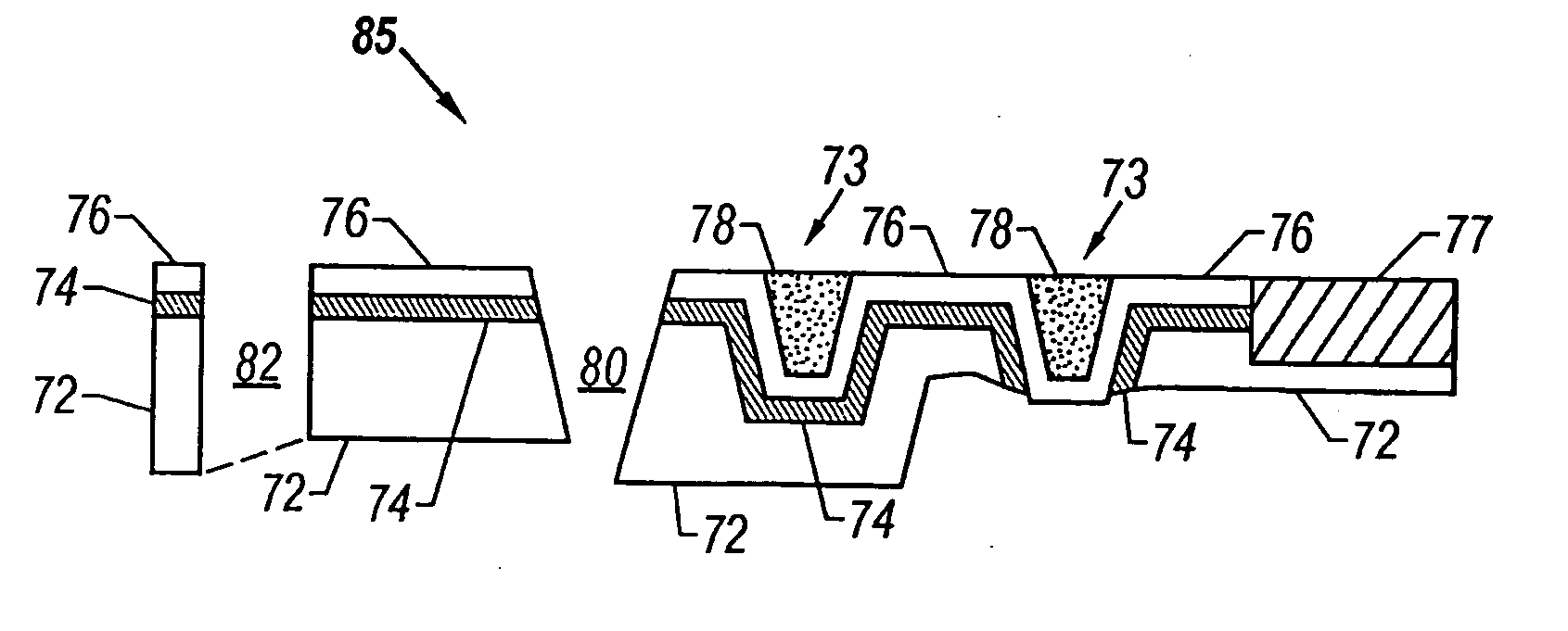
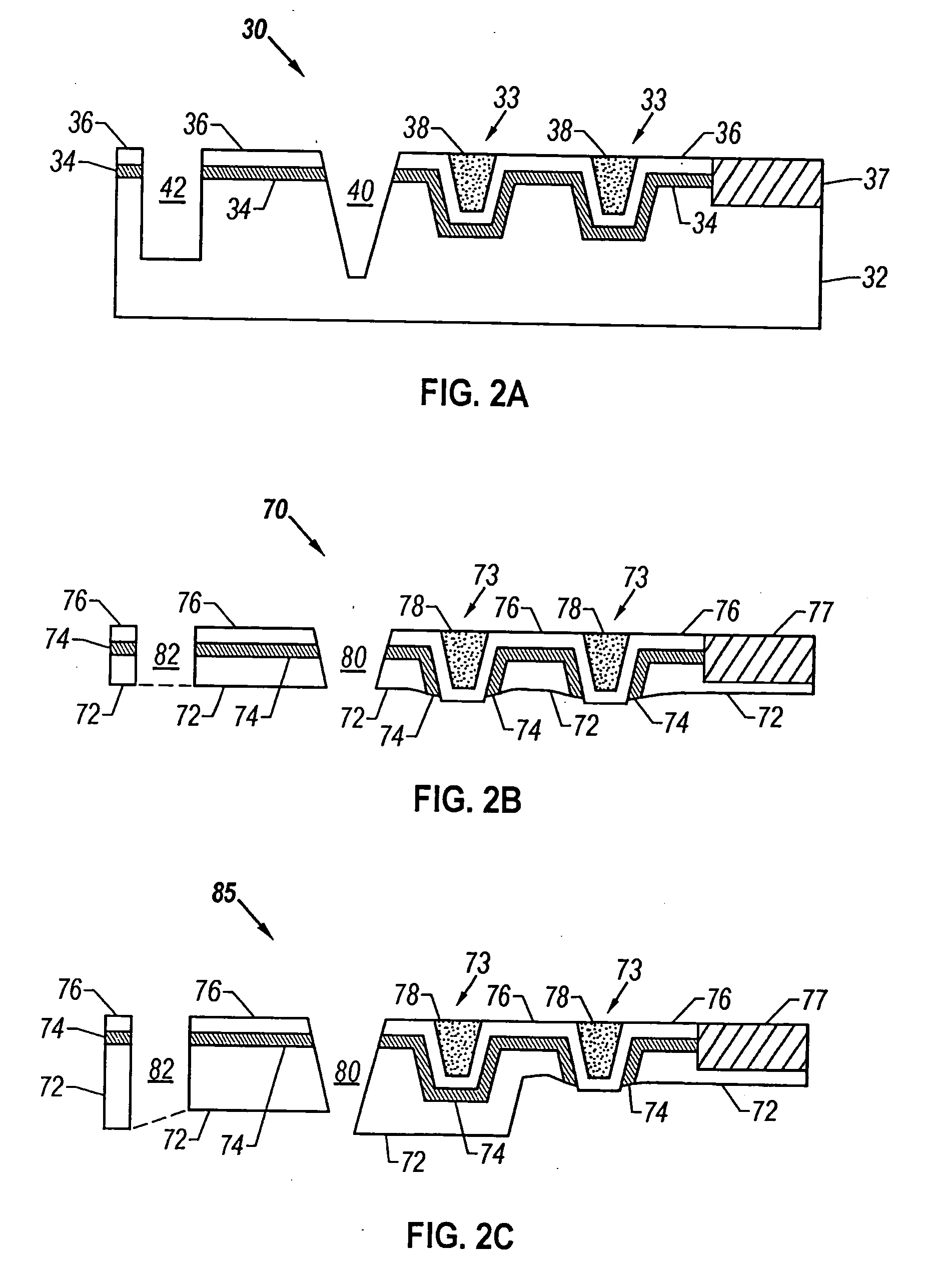
[0020] Another aspect of the invention may be found in a method of segregating IC chips contained within a wafer. The wafer may be first diced, grooved, notched, scored, or etched, among others, on a first side to form a groove, notch, hole, indentation, or channel, among others. The front side of the wafer may then be taped or laminated. Next, an etching process may be used on the backside of the wafer to thin the wafer to a thickness less than or equal to the depth of the groove, notch, hole, indentation, or channel. The etching portion of this method comprises using a magnetic mirror plasma etching technique and may further comprise a plasma etching technique, wet etching technique, dry etching technique, or a combination of those techniques, among others. The method may also be used to form holes or punch-throughs in the wafer or IC chip. These punch-throughs may, for example, allow electrical contact with front side circuitry. Alternately, they may be used as structural elements in MEMs. However, the holes or punch-throughs may have various uses.
[0021] A further aspect of the invention may be found in a method for simultaneously segregating IC chips contained within a wafer and exposing vias on the backside of an IC chip. Vias may be formed on the front side of the wafer with a first depth. In addition, the front side may be diced, grooved, scored, etched, or notched to second depth. The second depth may or may not be the same as the first depth. Next, the wafer may be taped or laminated. The backside of the wafer may then be etched to a depth that both exposes the vias and the groove, score, hole, indentation, or channel. The etching portion of this method comprises using a magnetic mirror plasma etching technique and may further comprise a plasma etching technique, wet etching technique, dry etching technique, or a combination of those techniques, among others. Another aspect of the invention may be found in pre-thinning a wafer with a conventional technique, followed by etching to expose vias, grooves, and or holes.
[0022] Other aspects of the invention may be found in methods for manufacturing IC chips, micro-electro-mechanical systems, and semiconductor wafers with low variance thickness among others.

