Semiconductor device manufacturing method

a manufacturing method and semiconductor technology, applied in the direction of semiconductor devices, basic electric elements, electrical appliances, etc., can solve the problems of unstable characteristics of withstanding voltage, increase of on resistance, and many other problems, to achieve the effect of preventing an on resistance from increasing, reducing production costs, and saving weigh

Inactive Publication Date: 2005-02-17
DENSO CORP
View PDF7 Cites 46 Cited by
  • Summary
  • Abstract
  • Description
  • Claims
  • Application Information

AI Technical Summary

Benefits of technology

[0013] This structure prevents an ON resistance from increasing due to horizontal misalignment of masking or vertical misalignment of depth control during forming a gate trench. Since the second semiconductor region directly connects with the body region, the second semiconductor region is not moved to floating electric potential. Furthermore an electric current passage can be shortened between the second semiconductor region and the body region. No necessity of independently disposing a p type silicon region for connecting the second semiconductor region and the body region leads to realization of downsizing, weight saving, and high integration in the semiconductor device.

Problems solved by technology

These manufacturing problems arise even at the present day when micro-fabrication is much progressed.
A characteristic of withstanding voltage may thereby become unstable.

Method used


Image

  • Semiconductor device manufacturing method
  • Semiconductor device manufacturing method
  • Semiconductor device manufacturing method

Examples


first embodiment

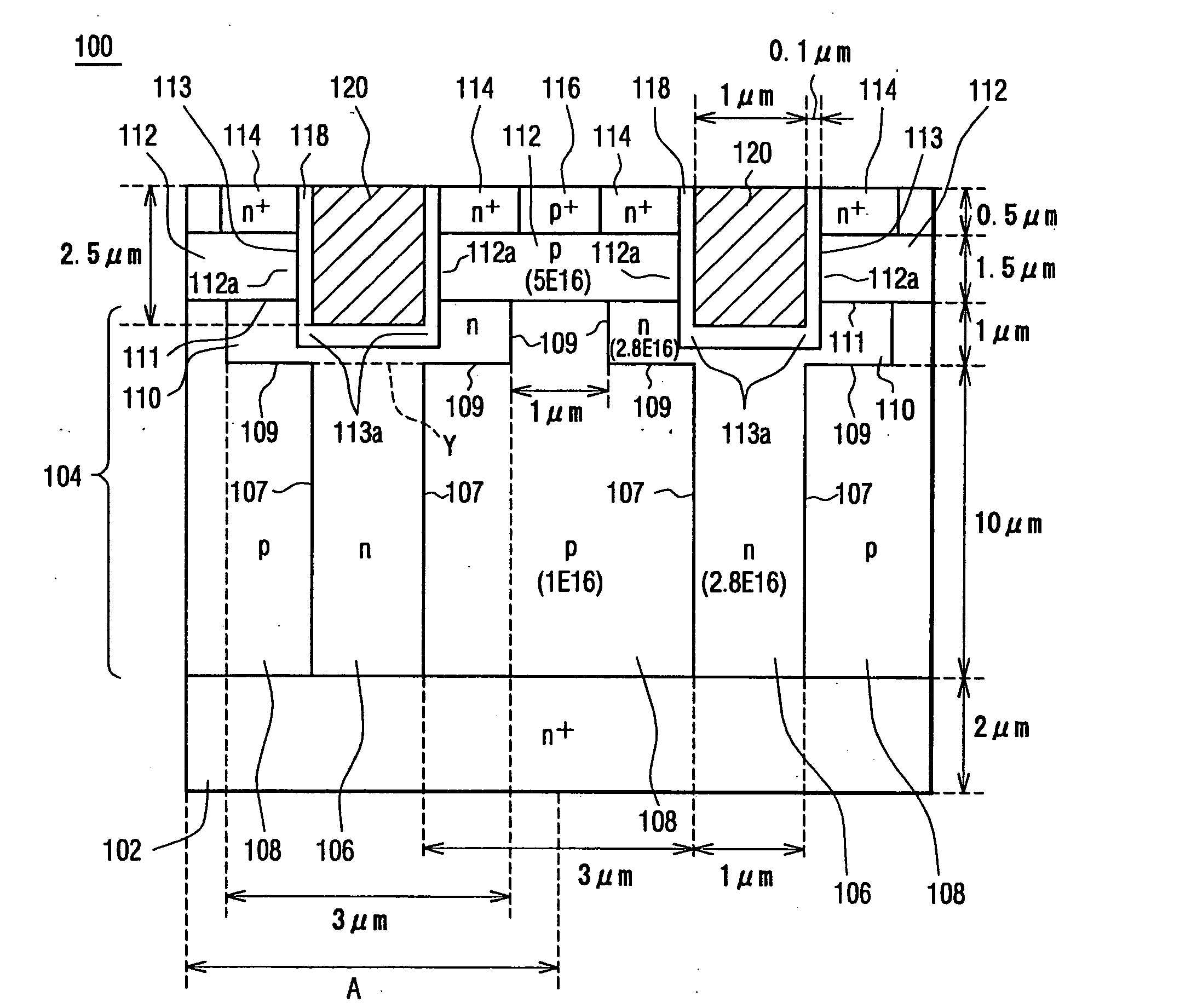
[0057] A vertical semiconductor device 100 of a first embodiment of the present invention is shown in a sectional view in FIG. 1. A width A shown in a lower area of FIG. 1 shows a unit structure that is repeatedly formed in a horizontal direction (from side to side) of FIG. 1.

[0058] The semiconductor device 100 forms metal oxide semiconductor (MOS) field effect transistor (FET) structure of a U trench type (U-shaped gate trench 113). The semiconductor device 100 is used for a motor of a vehicle, or a power converter or power control of electrical appliances for home use.

[0059] The semiconductor device 100 includes a drain region 102, a drift region 106, a silicon region 108, a body region 112, an upper silicon region 110, a source region 114, and a gate 120.

[0060] The drain region 102 is an n+ type (first conductivity type). It is 2 μm thick (vertical direction (from bottom to top) in FIG. 1).

[0061] The drift region 106 is an n type (first conductivity type) and connects with th...

second embodiment

[0121] A vertical semiconductor device 200 as a second embodiment is shown in a sectional view in FIG. 29. The vertical semiconductor device 200 includes an n− type upper silicon region 210 independently from an n type drift region 206. The n− type upper silicon region 210 has an n type impurity of 1 E 16 cm−3, while the n type drift region 206 has an n type impurity of 2.8 E 16 cm−3. It is thus favorable that the n type upper silicon region 210 has lower impurity concentration than the n type drift region 206. With an object that the n− type upper silicon region 210 should be occupied with the depletion layer during withstanding voltage, it is favorable that the n− type upper silicon region 210 has lower impurity concentration. By contrast, the n type drift region 206 is required to have low ON resistance in addition of high withstanding voltage, so that it favorably has high impurity concentration. The n− type upper silicon region 210 is assembled inside the p type body region 212...

third embodiment

[0128] A vertical semiconductor device 300 as a third embodiment is shown in a sectional view in FIG. 35. In the vertical semiconductor device 300, width (0.5 μm) of an n type drift region 306 is narrower than width (1 μm) of the n type drift region 106 of the first embodiment shown in FIG. 1. The n type drift region 306 has an n type impurity of 6.5 E 16 cm3. Width (3.5 μm) of a p type silicon region 308 is broader than width (3 μm) of the p type silicon region 108 of the first embodiment. The p type silicon region 308 has a p type impurity of 1.0 E 16 cm−3. Width (0.7 μm) of an n type upper silicon region 310 is narrower than width (3 μm) of the n type upper silicon region 110 of the first embodiment. Here, the n type upper silicon region 310 and the n type drift region 308 are formed as one uniform body with having a boundary at dotted line Y in FIG. 35.

[0129] Width (0.7 m) of the n type upper silicon region 310 is narrower than that (1.2 μm) of a gate trench 313. The n type upp...


PUM


Abstract

A semiconductor device includes: an n+ type drain region; an n type drift region that connects with the n+ type drain region; a p type body region; a n+ type source region that connects with the p type body region; and a gate electrode that is provided, with being covered by a gate insulation film, in a gate trench that penetrates the p type body region. The semiconductor further includes: a p type silicon region that adjoins the n type drift region; and an n type silicon region provided in a region almost including a carrier passage that connects the n type drift region and the p type body region. Here, the p type silicon region and the p type body region directly connect with each other.

Description

FIELD OF THE INVENTION [0001] The present invention relates to a semiconductor device and its manufacturing method. In particular, the semiconductor device is, for instance, used as MOS FET with having high withstanding voltage and low ON resistance. BACKGROUND OF THE INVENTION [0002] A semiconductor device in JP-A-2000-260984 is shown as a related art in FIG. 42. The semiconductor device 1 includes: an n+ type (first conductivity type) drain region 2; an n type (first conductivity type) drift region 6 connecting with the n+ type drain region 2; a p type (second conductivity type) body region 12; an n+ type source region 14 connecting with the p type body region 12; a gate electrode 20 filled with being covered by an insulation film 18 in a gate trench 13 that penetrates the p type body region 12; a p type silicon region (semiconductor region) 8 adjoining the n type drift region 6; and an n− type (first conductivity type) silicon region 11 covering the n type drift region 6 and the ...

Claims


Application Information

Patent Timeline
Patent Type & Authority Applications(United States)
IPC IPC(8): H01L21/336H01L29/06H01L29/78
CPCH01L29/7813H01L29/0634
Inventor YAMAGUCHI, HITOSHIHATTORI, YOSHIYUKI
Owner DENSO CORP
Why Eureka
Try Eureka