High voltage transistor and method of manufacturing the same

a high-voltage transistor and manufacturing method technology, applied in the field of semiconductor devices, can solve the problems of increasing the size of high-voltage transistors and the inability to apply the salicide process to embody high-speed logic transistors on the entire surface of wafers, and achieve the effect of reducing the transistor size and enforcing separation distan

Inactive Publication Date: 2005-02-17
SAMSUNG ELECTRONICS CO LTD
View PDF4 Cites 25 Cited by
  • Summary
  • Abstract
  • Description
  • Claims
  • Application Information

AI Technical Summary

Benefits of technology

[0013] The present invention provides a high voltage transistor having enough separation distance between a gate electrode and a high concentration drain region and having a layout not needing consideration of a misalign margin, thereby reducing the transistor size.
[0014] Also, the present invention provides a method of manufacturing a high voltage transistor to which a salicide process can be applied to improve a performance of the high voltage transistor used in a peripheral circuit.
[0033] In the present invention, since the salicide process can be performed on the entire surface of the peripheral circuit region together with the memory cell region, a current characteristic, that is, the performance of the high voltage transistor formed on the peripheral circuit region, can be improved. Further, the gate electrode of the high voltage transistor is formed as an asymmetric structure such that enough separation distance can be secured between the gate electrode and the high concentration junction of the drain region, thereby maintaining the high breakdown voltage. Additionally, since the insulating spacer is formed on both sidewalls of the gate electrode and then the high concentration implantation is performed in the self-alignment manner using the insulating spacer to form the source region and the drain region, the conventional misalign margin of the photolithography process does not need to be considered. Accordingly, the layout reduced in size corresponding to a design rule can be obtained with the conventional misalign margin. Furthermore, the source region and the drain region are formed as asymmetric structures with respect to the gate electrode such that the area of the source region can be minimized thereby reducing the transistor in size.

Problems solved by technology

This causes the high voltage transistor to increase in size.
However, as exemplified in the conventional art of FIG. 1, if the photoresist pattern is used at the peripheral circuit region to secure the separation distance (X1) between the gate electrode 20 and the high concentration drain region 16b, it is impossible to apply the salicide process for embodying a high speed logic transistor to the entire surface of a wafer.

Method used


Image

  • High voltage transistor and method of manufacturing the same
  • High voltage transistor and method of manufacturing the same
  • High voltage transistor and method of manufacturing the same

Examples


Embodiment Construction

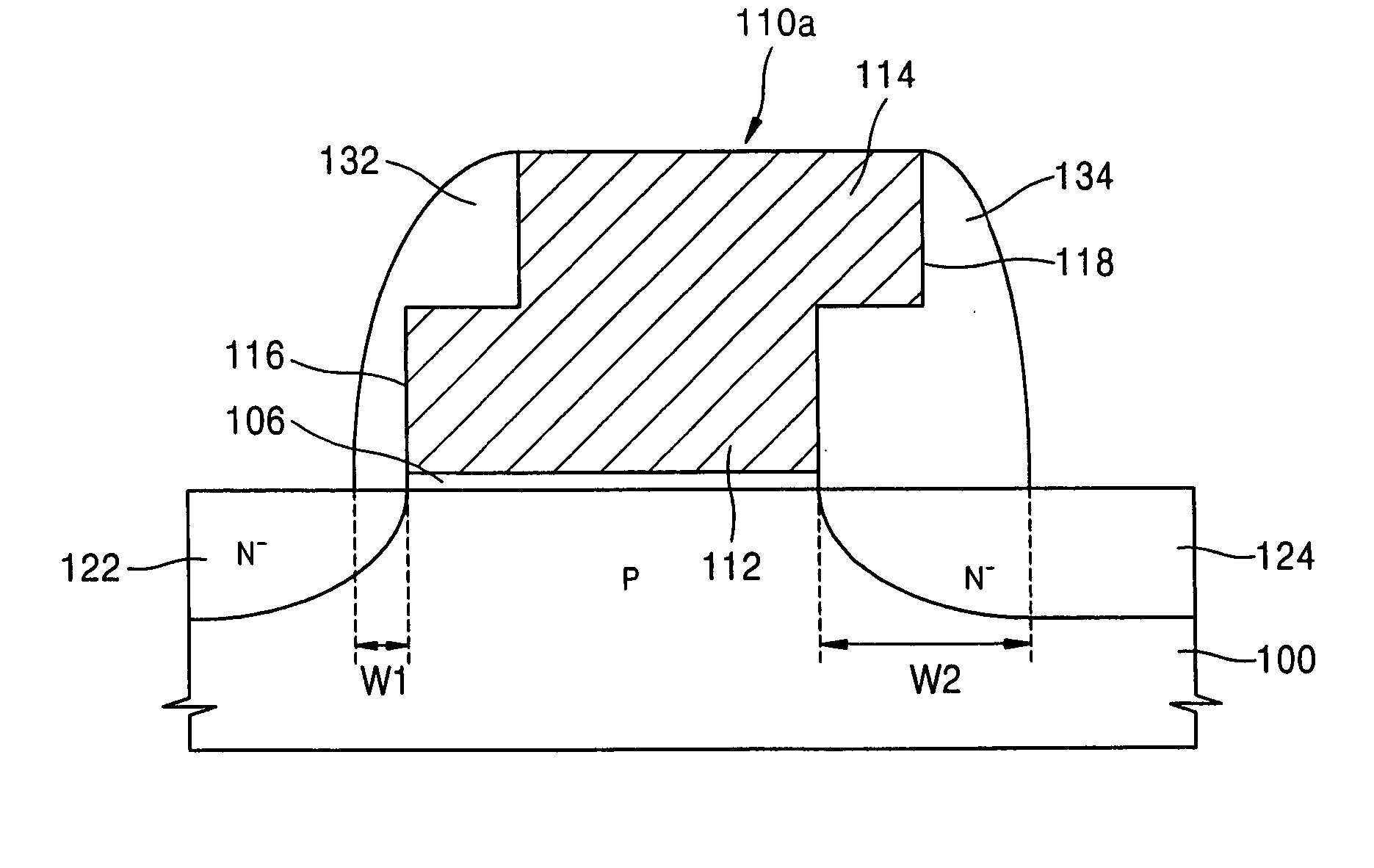
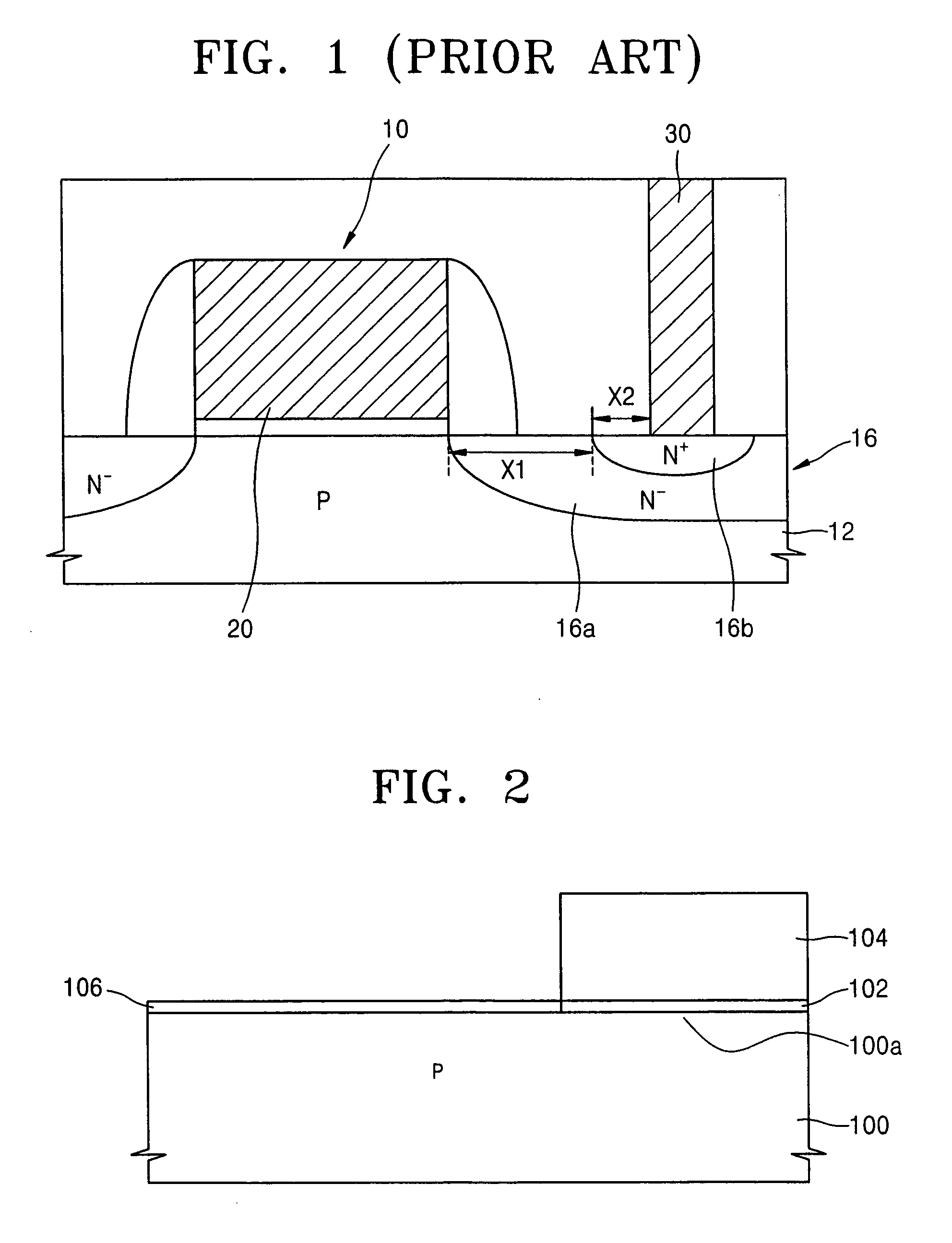
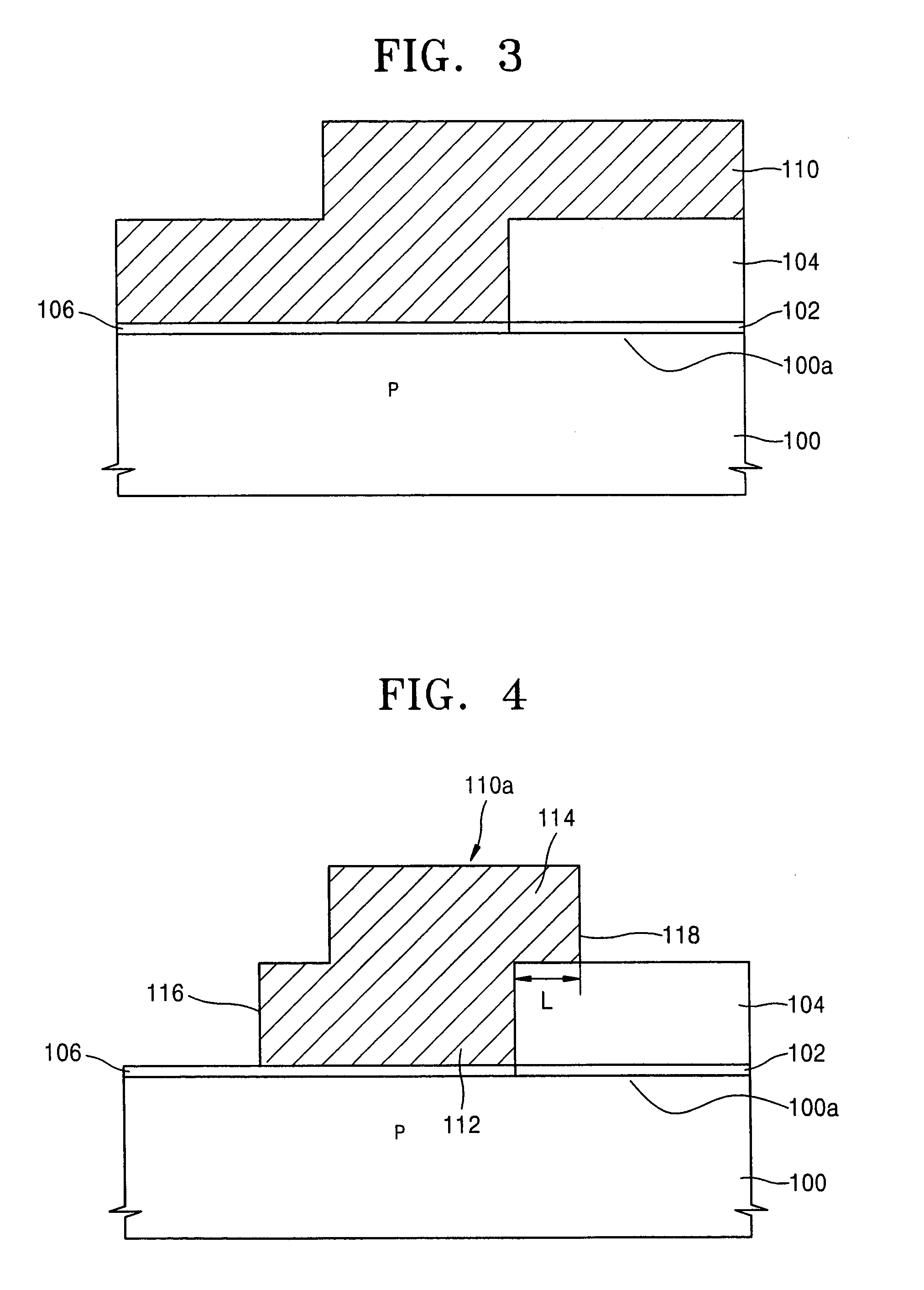
[0037] The present invention will now be described more fully with reference to the accompanying drawings, in which exemplary embodiments of the invention are shown. In the drawings, the thicknesses of layers and regions are exaggerated for clarity.

[0038]FIGS. 2 through 8 are sectional views illustrating a high voltage transistor and a process sequence of a method of manufacturing a high voltage transistor according to an embodiment of the present invention.

[0039] The semiconductor substrate includes a memory cell region of a nonvolatile memory device having a plurality of memory cells arrayed in matrix, and the peripheral circuit region. Further, in this embodiment, an NMOS transistor on a P-type semiconductor substrate is exemplified. However, the present invention is not limited to this embodiment, but can be applied to a case where the NMOS transistor can be formed in a P-type well region formed in the semiconductor substrate and can be identically applied to a case where a PM...


PUM


Abstract

The present invention relates to a high voltage transistor and method of manufacturing the same. The high voltage transistor includes: a channel region which is formed in a semiconductor substrate; a gate insulating film which is formed on the channel region of the semiconductor substrate; a low concentration source region and a low concentration drain region having the channel region interposed therebetween and each being formed in the semiconductor substrate; a high concentration source region which is formed to be spaced away from the channel region by a first distance; a high concentration drain region which is formed to be spaced away from the channel region by a second distance that is larger than the first distance; a gate electrode which has a gate bottom portion interfacing with the gate insulating film over the channel region, and a gate top portion integrated with the gate bottom portion and protruding by a predetermined length from a top of the gate bottom portion to extend over the low concentration drain region; a first metal silicide layer which is formed on the high concentration source region; and a second metal silicide layer which is formed on the high concentration drain region.

Description

BACKGROUND OF THE INVENTION [0001] This application claims the priority of Korean Patent Application No. 2003-55363, filed on Aug. 11, 2003, in the Korean Intellectual Property Office, the contents of which are incorporated herein in their entirety by reference. [0002] 1. Field of the Invention [0003] The present invention relates to a semiconductor device and a method of manufacturing the same, and more particularly, to a high voltage transistor used in a peripheral circuit of a flash memory device or an Electrically Erasable and Programmable Read Only Memory (EEPROM) device that is a nonvolatile memory device operating at a high voltage, and a method of manufacturing the same. [0004] 2. Description of the Related Art [0005] When a semiconductor integrated circuit directly controls an external system using a high voltage, the integrated circuit requires a high voltage control device to which the external system directly applies the high voltage, and a circuit needing a high breakdo...

Claims


Application Information

Patent Timeline
Patent Type & Authority Applications(United States)
IPC IPC(8): H01L21/265H01L29/41H01L21/28H01L21/336H01L21/8247H01L27/115H01L29/417H01L29/423H01L29/78H01L29/788H01L29/792H01L31/0328
CPCH01L21/26586H01L21/28114H01L29/7835H01L29/665H01L29/66659H01L29/42376H01L29/78
Inventor YU, TAE-KWANGJEON, HEE-SEOGYOON, SEUNG-BEOMKIM, YONG-TAE
Owner SAMSUNG ELECTRONICS CO LTD
Why Eureka
Try Eureka