Multi-chip package device with heat sink and fabrication method thereof

a technology of multi-chip package devices and heat sinks, which is applied in the direction of semiconductor devices, semiconductor/solid-state device details, electrical apparatus, etc., can solve the problems of increasing the processing speed of semiconductors, reducing the processing efficiency of semiconductors, so as to prevent delamination, cracking and warpage of the package device

Inactive Publication Date: 2005-02-17
SILICONWARE PRECISION IND CO LTD
View PDF7 Cites 20 Cited by
  • Summary
  • Abstract
  • Description
  • Claims
  • Application Information

AI Technical Summary

Benefits of technology

[0019] The primary advantage achieved by the multi-chip package device according to the present invention is that, the provision of the hollow part in the heat sink allows thermal stresses produ

Problems solved by technology

And the enhancement in the processing speed is usually accompanied by a large amount of heat generated when the chip executes the computation.
Therefore, the conventional multi-chip package device that lacks an effective heat sink is not suitable to be packaged

Method used


Image

  • Multi-chip package device with heat sink and fabrication method thereof
  • Multi-chip package device with heat sink and fabrication method thereof
  • Multi-chip package device with heat sink and fabrication method thereof

Examples


Embodiment Construction

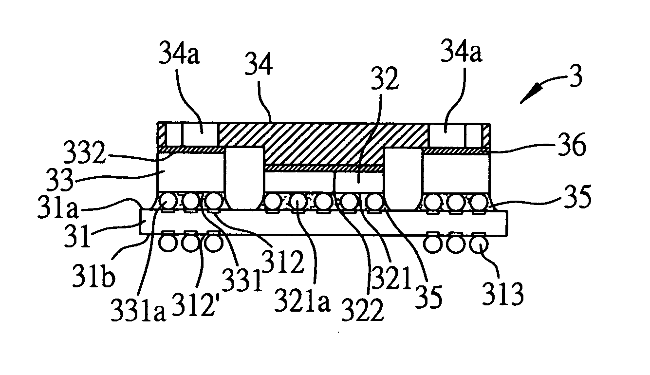
[0031] As shown in FIGS. 4a, 4b and 4c, a multi-chip package device 3 proposed by the present invention comprises a chip carrier 31, a first chip 32, a plurality of semiconductor packages 33, and a heat sink 34.

[0032] The chip carrier 31 has a first surface 31a and a second surface 31b opposite to the first surface 31a. A plurality of conductive traces (not shown) are formed on the first surface 31a and the second surface 31b respectively, wherein bond pads 312 are formed at terminals of the conductive traces on the first surface 31a, and bond pads 312′ are formed at terminals of the conductive traces on the second surface 31b and bonded with an array of solder balls 313 that mediate electrical connection of the package device 3 with an external device (not shown).

[0033] The first chip 32 has an active surface 321 and an inactive surface 322. The first chip 32 is mounted on the chip carrier 31 in a flip-chip manner that, a plurality of bumps 321a formed on the active surface 321 a...


PUM


Abstract

A multi-chip package device with heat sink and a fabrication method thereof are proposed. At least one first chip and at least one semiconductor package are mounted on and electrically connected to a chip carrier. Then, a heat sink is mounted via an adhesion layer to the first chip and the semiconductor package. In addition, at least one hollow part extending through the heat sink is formed in an area of the heat sink free of contact from the first chip and the semiconductor package, in order to release thermal stresses produced from the heat sink. Thereby, the package device can be prevented from being damaged during the reliability test process, and a product yield is thereby promoted.

Description

FIELD OF THE INVENTION [0001] The present invention relates to multi-chip package devices and fabrication methods thereof, and more particularly, to a multi-chip package device with a heat sink, which can release thermal stresses from the heat sink, and a fabrication method of the package device. BACKGROUND OF THE INVENTION [0002] With a growing demand for minimized electrical products with high operation speed, a semiconductor package device is presented with a Multi Chip Module (MCM) to improve performance and capacity of a single package device and to meet requirements for the electrical product with a minimal size, maximal capacity and high operation speed. As this package device has a reduced overall size and improved electrical functions, it becomes one of the main trends among the packaged products. [0003] For example of a graphic adapter that is installed in a Personal Computer (PC) to rapidly process and display graphics, particularly 3-dimensional (3D) graphics, besides a ...

Claims


Application Information

Patent Timeline
IPC IPC(8): H01L23/367
CPCH01L23/367H01L2924/15311H01L2224/73253H01L2224/73204H01L2224/32245H01L2224/16225H01L2224/32225H01L2924/00
Inventor HUANG, CHIEN-PING
Owner SILICONWARE PRECISION IND CO LTD
Why Eureka
Try Eureka