Device with low-k dielectric in close proximity thereto and its method of fabrication

a dielectric and close proximity technology, applied in the direction of semiconductor devices, semiconductor/solid-state device details, electrical apparatus, etc., can solve the problems of increasing parasitic capacitance, short-channel effect, and bottleneck, and achieve the effect of reducing parasitic capacitan

Inactive Publication Date: 2005-02-17
TAIWAN SEMICON MFG CO LTD
View PDF28 Cites 236 Cited by
  • Summary
  • Abstract
  • Description
  • Claims
  • Application Information

AI Technical Summary

Benefits of technology

[0009] A broad object of the invention is to provide a semiconductor device having an ultra deep sub-micron feature length and its method of fabrication.
[0010] Another object of the invention is to provide an ultra deep sub-micron device and its method of fabrication whereby scaling issues of the parasitic capacitance between the gate and the contact plug are addressed.
[0011] A further object of the invention is to provide an ultra deep sub-micron device and its method of fabrication whereby scaling issues of the parasitic capacitance between two adjacent contact plugs are addressed.

Problems solved by technology

However, various problems are caused as a result of the reduction in size of the elements.
For example, the shortening of the channel length achieves the effect of lowering the channel resistance on the one hand but, on the other, gives rise to the problem that a short-channel effect is brought about.
An unrecognized problem is the increase of the parasitic capacitance between the gate electrode and the adjacent conductive plug used to connect the transistor, which however, will become a bottleneck in ultra-miniaturization of devices according to the present inventors' investigation.
Considerable work has been done to reduce the junction capacitance of the source / drain, but has not addressed the problems associated with the parasitic capacitance between the gate electrode and the conductive plug or of that between adjacent plugs.

Method used


Image

  • Device with low-k dielectric in close proximity thereto and its method of fabrication
  • Device with low-k dielectric in close proximity thereto and its method of fabrication

Examples


first embodiment

[0034] First Embodiment

[0035] A preferred embodiment of the present invention is now described in detail with reference to FIG. 1.

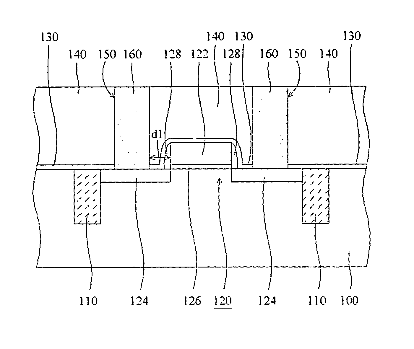
[0036]FIG. 1 is a schematic cross-section showing a semiconductor substrate 100 having a field effect MOS transistor 120 with a low-k dielectric layer 140 in close proximity thereto. The preferred substrate 100 is composed of P type single-crystal silicon with a crystallographic orientation, and may contains defective semiconductor lattice in the channel region of the MOS transistor 120 to increase drive current. For example, a SiGe epitaxial layer may be grown for mobility enhancement.

[0037] The MOS transistor 120 is formed in an active device area isolated by isolation elements such as the well-known shallow trench isolation (STI) structures 110 as shown. The MOS transistor includes a gate electrode 122 overlying the substrate with a gate dielectric 126 interposed therebetween, and a pair of source / drain regions 124 formed in the substrate oppositely...

second embodiment

[0045] Second Embodiment

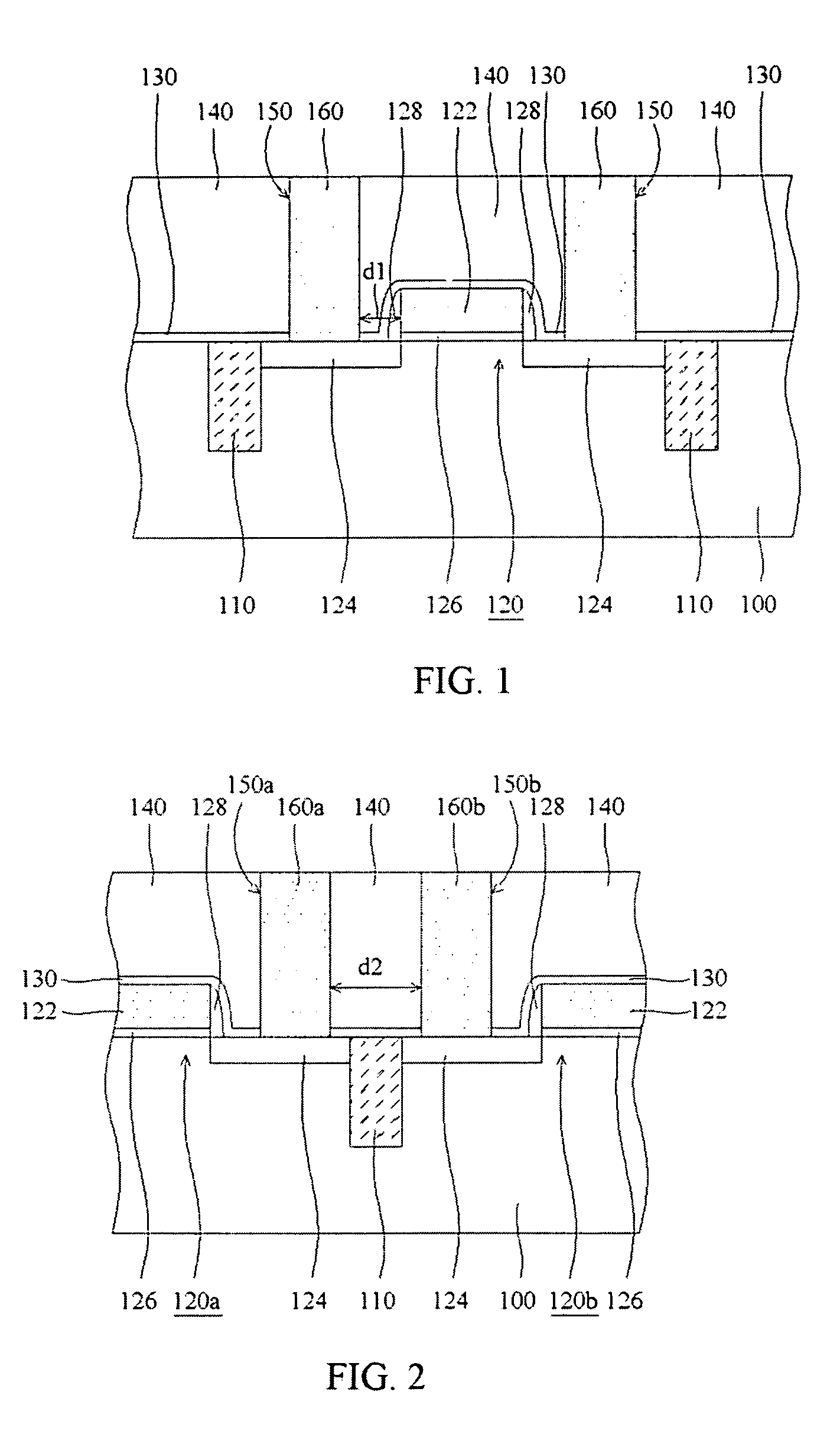
[0046]FIG. 2 shows another embodiment of the invention, in which like numbers from the first described embodiment are utilized where appropriate. Two closely spaced field effect MOS transistors 120a, 120b are formed on a semiconductor substrate using known processes, isolated by a STI 110 therebetween. After a conformal buffer layer 130 (optional) and a blanket low-k dielectric layer 140 as in the first embodiment are formed, two contact openings 150a, 150b are defined through the low-k dielectric layer 140 between the two transistors to respectively expose one of the source / drain regions 124 of each transistor. Thereafter, electrically conductive materials are embedded in the contact openings 150a, 150b, thereby forming two adjacent conductive plugs 160a, 160b to respectively make electrical contact to each of the MOS transistors 120a, and 120b.

[0047] As shown in FIG. 2, the low-k dielectric material 140 reduces the parasitic capacitance between the two adj...


PUM


Abstract

A semiconductor device with a low-k material in close proximity thereto and its fabrication method. The device includes a gate electrode overlying a substrate. An electrically conductive plug is provided immediately adjacent to the gate electrode and making electrical contact to the device. A low-k dielectric material is disposed in the space between the gate electrode and the electrically conductive plug whereby reducing the parasitic capacitance. Thus, higher density of devices can be formed without decreasing operating speed.

Description

BACKGROUND OF THE INVENTION [0001] 1. Field of the Invention [0002] The invention relates to semiconductor manufacturing, and more particularly to a semiconductor device with a low-k (low dielectric constant) material in close proximity thereto and a method of manufacturing the same. [0003] 2. Description of the Related Art [0004] Semiconductor device geometries have dramatically decreased in size since such devices were first introduced several decades ago. Today's wafer fabrication plants are routinely producing devices having 0.18 μm and even 0.15 μm feature sizes, and tomorrow's plants will soon be producing devices with even smaller geometries. [0005] However, various problems are caused as a result of the reduction in size of the elements. For example, the shortening of the channel length achieves the effect of lowering the channel resistance on the one hand but, on the other, gives rise to the problem that a short-channel effect is brought about. Further, as a result of the r...

Claims


Application Information

Patent Timeline
Patent Type & Authority Applications(United States)
IPC IPC(8): H01L21/336H01L21/44H01L21/768H01L29/78
CPCH01L29/6656
Inventor HU, CHENMINGTANG, DENNYTSENG, HORNG-HUEI
Owner TAIWAN SEMICON MFG CO LTD
Why Eureka
Try Eureka