
Monolithically integrated microwave guide component for radio frequency overcoupling

Inactive Publication Date: 2005-02-17
TELEFON AB LM ERICSSON (PUBL)
View PDF2 Cites 0 Cited by
  • Summary
  • Abstract
  • Description
  • Claims
  • Application Information

AI Technical Summary

Benefits of technology

[0006] In comparison, the monolithically integrated microwave guide component in accordance with the invention provides the advantage that a compensation on coupling out RF signals is achieved in a simple manner. Since the microwave guides—of both the chip and the carrier—each have an integrated compensation structure in the contact region, the production of the RF coupling out can take place in a simple manner and an electrical design of the contact region can take place at the same time in such a way that a compensation of reflections is possible.
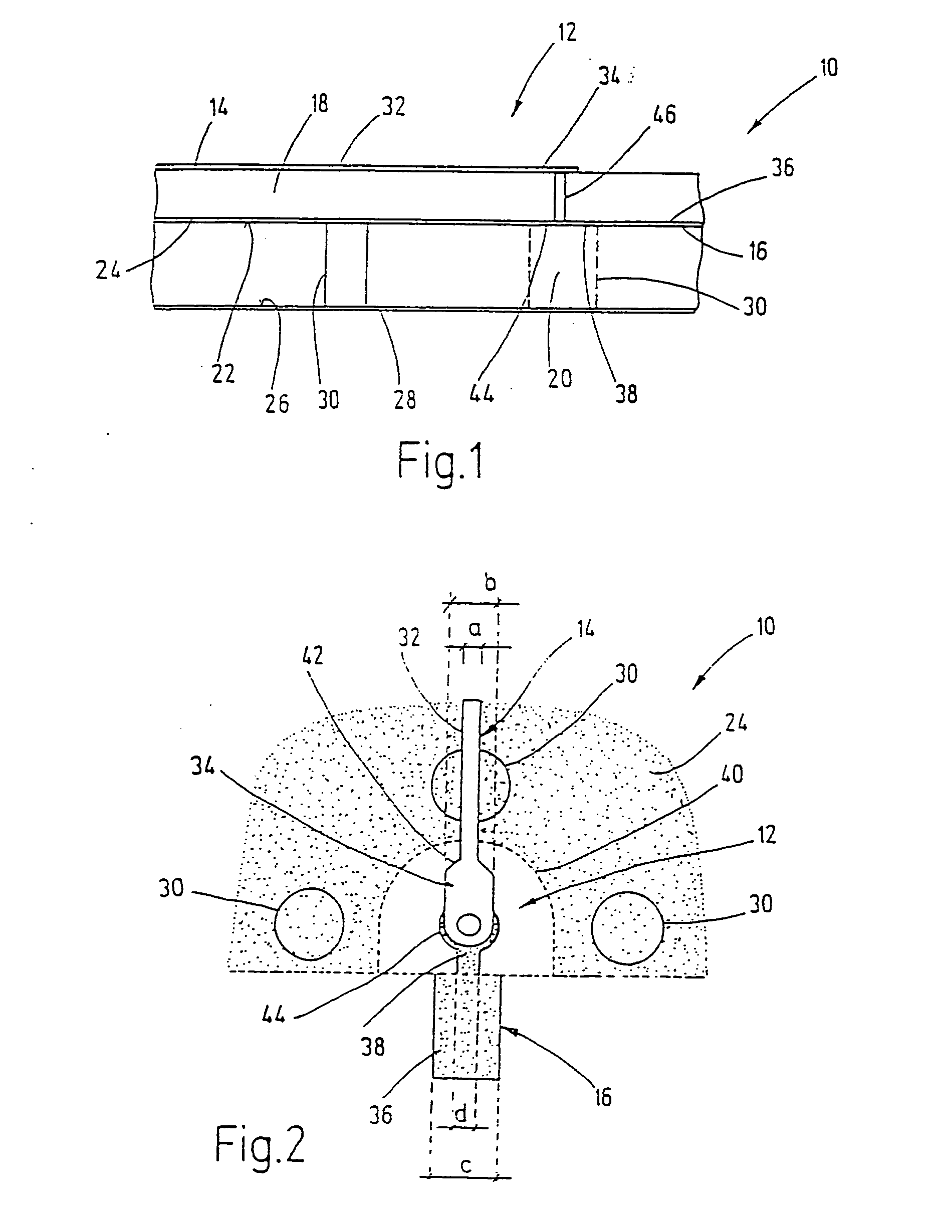
[0007] In one embodiment of the invention, provision is made for the compensation structures to be formed by line sections of the microwave guides which have a line width matched to the transition. The compensation structure can be hereby be integrated in a simple manner by specifying the layout of the microwave guides in the contacting region. It is in particular provided that the microwave guide associated with the chip forms a capacitively acting line section in the contact region and that the microwave guide associated with the carrier forms an inductively acting line section in the contact region. A compensation can be achieved by interaction of these line sections in the contact region with the grounding arrangement of the microwave guide component such that the line structure of the coupling out of RF signals corresponds to that of a 50 ohm standard microwave guide with sufficient accuracy.

Problems solved by technology

In this connection, it is disadvantageous that such a coupling out of high frequency electromagnetic waves leads, in particular with frequencies above 10 GHz, to increased reflections due to the inductance of the coupling out line.
As a rule, this requires high space requirements on the chip.
It is furthermore disadvantageous that due to the short wavelength associated with the high frequencies in assembly tolerances between the chip and carrier, or between the line structures and the coupling out line, result in the formation of parasitic elements (capacitances, inductances), which make compensation more difficult.
With such a via, the reflections caused by the usual bon connection or ribbon connection are admittedly avoided, but the problem of the compensation with the coupling out of RF signals remains unsolved.

Method used


Image

  • Monolithically integrated microwave guide component for radio frequency overcoupling
  • Monolithically integrated microwave guide component for radio frequency overcoupling

Examples


Embodiment Construction

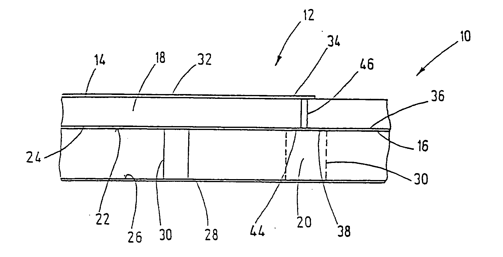
[0012] Referring now to the drawings, and more particularly to FIG. 1, there is shown a monolithically integrated microwave guide component 10 in a longitudinal section. Contact region 12 is shown of a first microwave guide 14 with a second microwave guide 16. Microwave guide 14 is arranged on a chip 18, for example on a GaAs (gallium arsenide) chip. Chip 18 has, for example, a thickness of 100 μm. Second microwave guide 16 is arranged on a carrier 20, for example an Al2O3 (aluminum oxide) substrate. Carrier 20 has, for example, a thickness of 254 μm. An upper side 22 of carrier 20 carries a metallic coating 24, whereas a lower side 26 on carrier 20 carries a metallic coating 28. Metallic coatings 24 and 28 are galvanically connected via through-contacts (or vias) 30 indicated here. Metallic coatings 24 and 28 serve in a known manner to make available a ground potential for circuits integrated into microwave guide component 10 which are not shown individually. These can, for example...


PUM


Abstract

A monolithically integrated microwave guide component for overcoupling high frequencies includes a first micro-waveguide that is structured on a micro-waveguide chip, and comprises a second micro-waveguide that is structured on a carrier substrate. The microwave guides are contacted to one another by a chip through-plating. The microwave guides each include, in the contact region, an integrated compensating structure that serves to compensate for reflections.

Description

BACKGROUND OF THE INVENTION [0001] 1. Field of the Invention [0002] The present invention relates to a monolithically integrated microwave guide component. [0003] 2. Description of the Related Art [0004] Microwave guide components of the generic kind are known. These serve for the coupling in or out of electromagnetic waves of a high frequency which are supplied via a microwave guide. Such microwave guide components consist of a chip in which a conductor configured as a strip line or as a micro-strip line is integrated. This conductor is applied as is known, to the upper side of the chip. Further circuit components, for example, amplifiers. oscillators or the like, can be integrated inside the chip. The chip is arranged on or next to a carrier which likewise has a conductor designed as a strip line or a micro-strip line for the electromagnetic waves. To connect the conductor structures of the chip and of the carrier to one another, it is known to contact these to one another via a b...

Claims


Application Information

Patent Timeline
IPC IPC(8): H01P1/04H01P3/08H01P5/00H03H7/38
CPCH01P1/047
Inventor KERN, STEFANGERHARD, GREGOR
Owner TELEFON AB LM ERICSSON (PUBL)
Learn More