Device threshold control of front-gate silicon-on-insulator mosfet using a self-aligned back-gate

a technology of silicon-on-insulator mosfet and device threshold control, which is applied in the direction of semiconductor devices, electrical devices, transistors, etc., can solve the problems of reducing supply and threshold voltage, increasing gate to source/drain capacitance, and suffering performance losses that will eventually reach the limit of diminishing returns. , to achieve the effect of enhancing device and circuit performance and minimizing capacitan

Inactive Publication Date: 2005-02-17
GLOBALFOUNDRIES INC
View PDF13 Cites 69 Cited by
  • Summary
  • Abstract
  • Description
  • Claims
  • Application Information

AI Technical Summary

Benefits of technology

[0008] The present invention provides SOI CMOS technology whereby a polysilicon, i.e., polySi, back-gate is used to control the threshold voltage of the front-gate device, and the nMOS and PMOS back-gates are switched independently of each other and the front gates. Specifically, the prese...

Problems solved by technology

Simultaneous reduction of supply and threshold voltages for low-power silicon-on-insulator (SOI) CMOS designs without suffering performance losses will eventually reach the limit of diminishing returns as static power dissipation becomes a significant portion of the total power equation.
Unfortunately, such a thin back-gate dielectric results in an increase in gate to source/drain capacitance;...

Method used


Image

  • Device threshold control of front-gate silicon-on-insulator mosfet using a self-aligned back-gate
  • Device threshold control of front-gate silicon-on-insulator mosfet using a self-aligned back-gate
  • Device threshold control of front-gate silicon-on-insulator mosfet using a self-aligned back-gate

Examples


Embodiment Construction

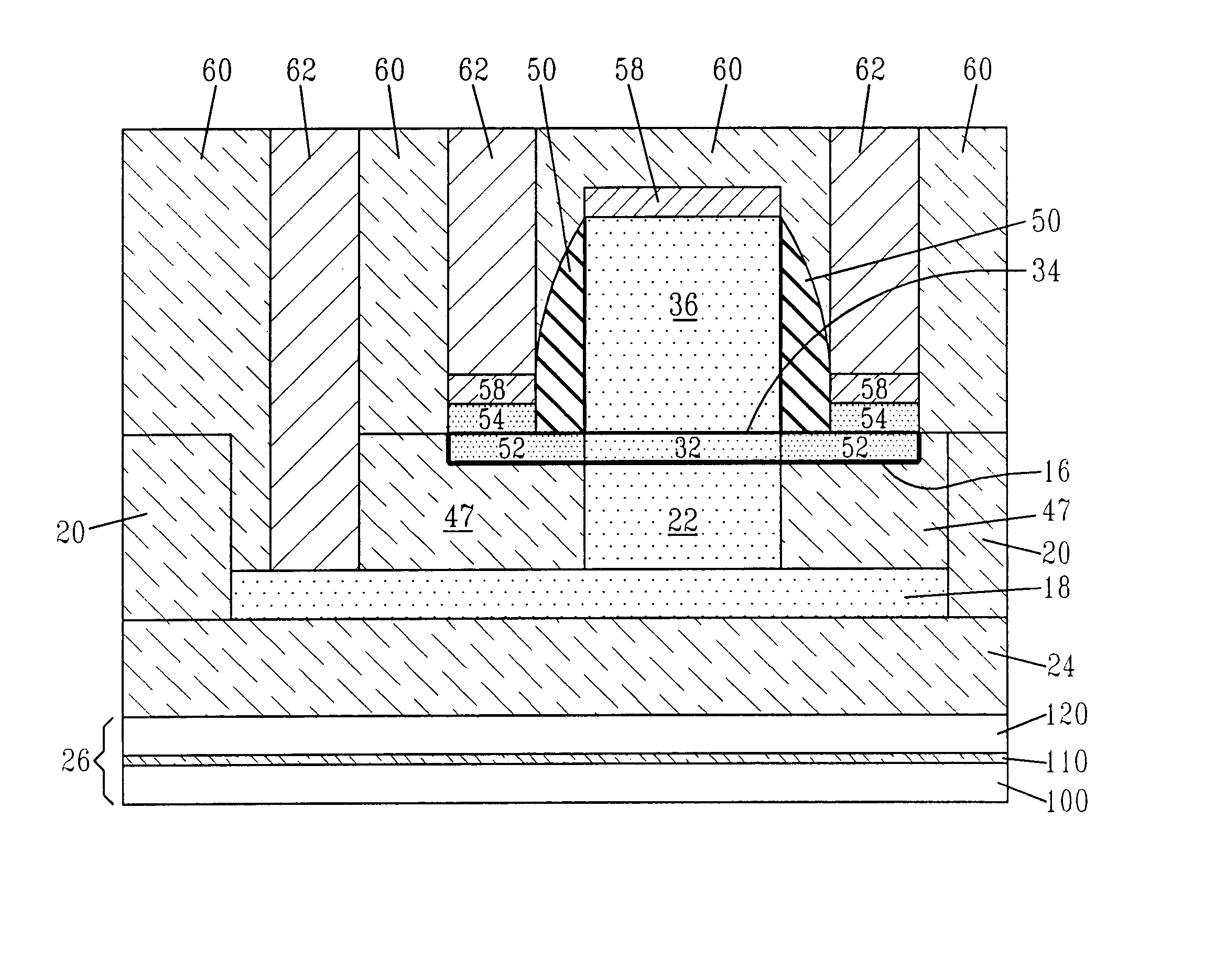
[0034] The present invention, which provides a method of fabricating a back-gated fully depleted CMOS device in which the back-gate controls the threshold voltage of the front-gate, will now be described in greater detail by referring to the drawings that accompany the present application. In the accompanying drawings, like and / or corresponding elements are referred to by like reference numerals.

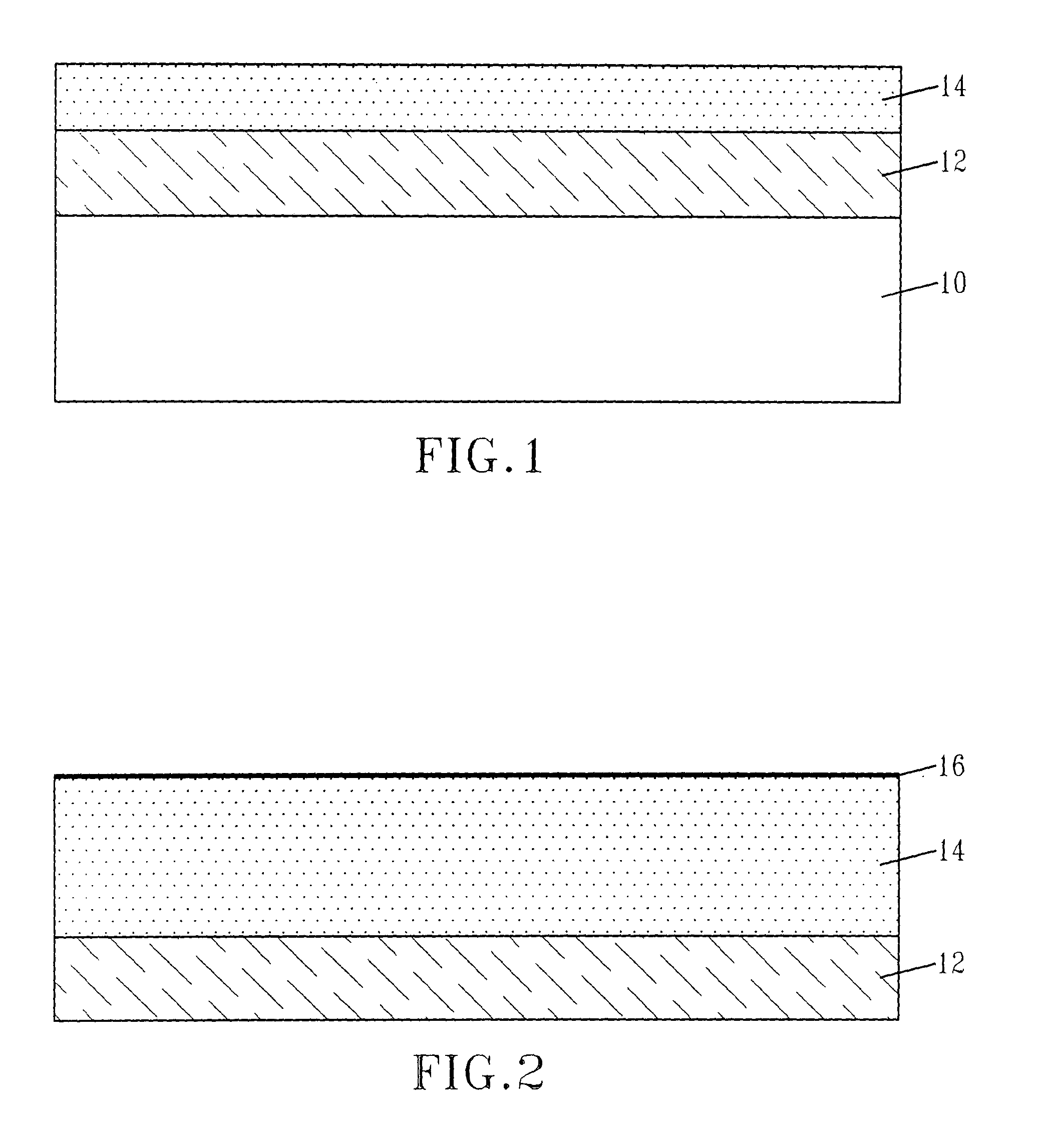
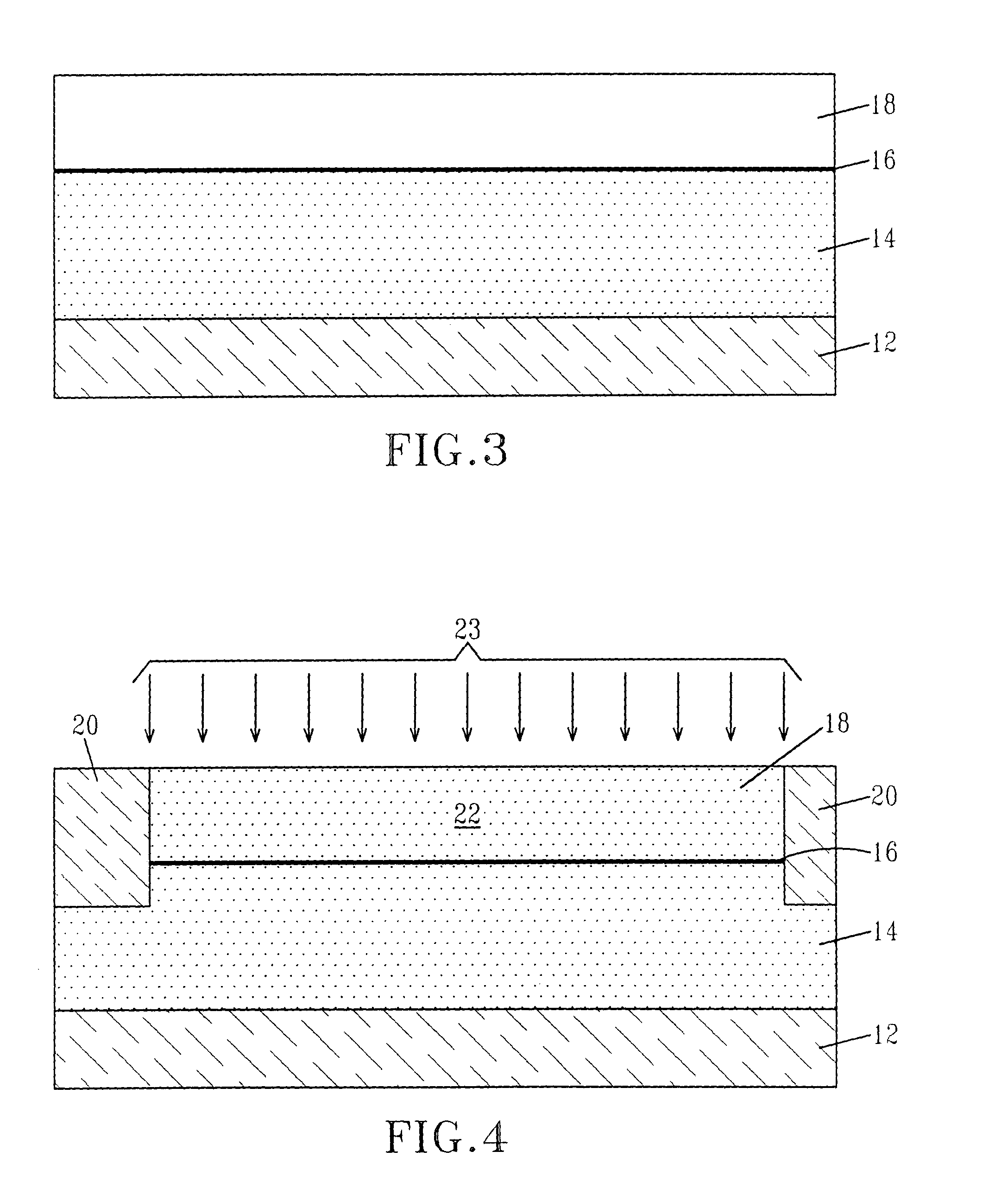
[0035]FIG. 1 illustrates an initial SOI substrate that can be employed in the present invention. The terms “SOI substrate” and “SOI wafer” are used interchangeably in the present application. Specifically, the initial SOI substrate or wafer of FIG. 1 comprises buried oxide layer 12 that electrically isolates Si-containing substrate 10 from Si-containing layer 14. Si-containing layer 14 is the SOI layer in which active device regions can be formed therein. The term “Si-containing” as used herein denotes a semiconductor material that includes at least silicon. Illustrative examples of such Si...


PUM


Abstract

The present invention provides SOI CMOS technology whereby a polysilicon back-gate is used to control the threshold voltage of the front-gate device, and the nMOS and pMOS back-gates are switched independently of each other and the front gates. Specifically, the present invention provides a method of fabricating a back-gated fully depleted CMOS device in which the device's back-gate is self-aligned to the device's front-gate as well as the source/drain extension. Such a structure minimizes the capacitance, while enhancing the device and circuit performance. The back-gated fully depleted CMOS device of the present invention is fabricated using existing SIMOX (separation by ion implantation of oxygen) or bonded SOI wafers, wafer bonding and thinning, polySi etching, low-pressure chemical vapor deposition and chemical-mechanical polishing.

Description

RELATED APPLICATIONS [0001] This application is related to co-pending and co-assigned U.S. patent application Ser. No. 10 / 235,169, filed Sep. 5, 2002, U.S. patent application Ser. No. 10 / 235,147, filed Sep. 5, 2002, and U.S. patent application Ser. No. 09 / 778,335, filed Feb. 7, 2001.FIELD OF THE INVENTION [0002] The present invention relates to semiconductor device manufacturing, and more particularly to a method of fabricating a fully depleted complementary metal oxide semiconductor (CMOS) device that includes a back-gate that is self-aligned to the front gate as well as the source / drain extensions. BACKGROUND OF THE INVENTION [0003] Simultaneous reduction of supply and threshold voltages for low-power silicon-on-insulator (SOI) CMOS designs without suffering performance losses will eventually reach the limit of diminishing returns as static power dissipation becomes a significant portion of the total power equation. In order to meet the opposing requirements of high-performance du...

Claims


Application Information

Patent Timeline
IPC IPC(8): H01L21/336H01L21/762H01L29/786
CPCH01L21/76256H01L21/76275H01L29/78696H01L29/78648H01L29/78654H01L29/66772H01L21/18
Inventor DENNARD, ROBERT H.HAENSCH, WILFRIED E.HANAFI, HUSSEIN I.
Owner GLOBALFOUNDRIES INC
Why Eureka
Try Eureka