

Method for producing polycrystalline silicon germanium and suitable for micromachining
- Summary
- Abstract
- Description
- Claims
- Application Information
AI Technical Summary
Benefits of technology
Problems solved by technology
Method used
Image

Examples
example 4
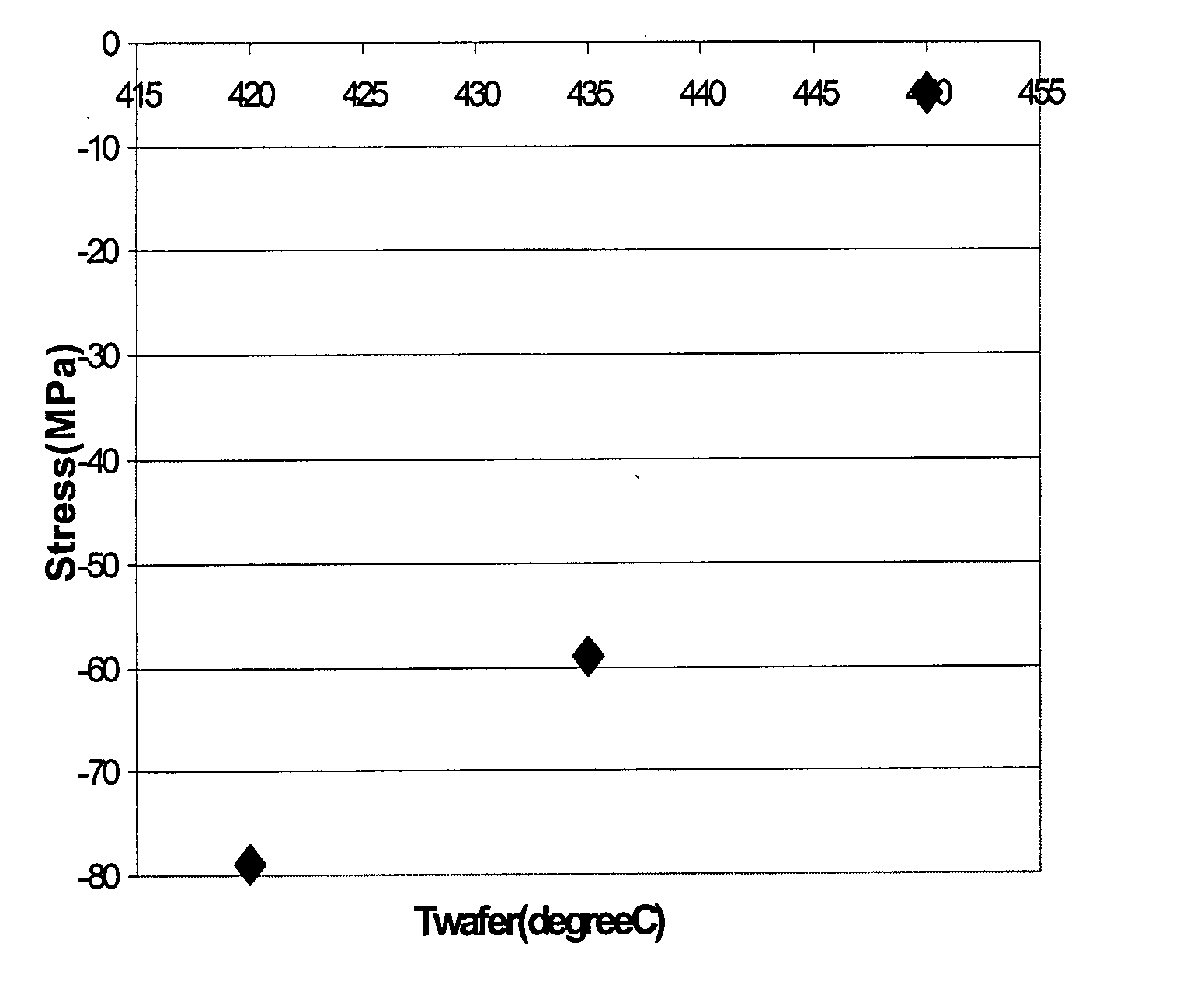
Films at 450° C.
Different variations of the process of preferred embodiments were investigated by varying the silane flow rates and deposition temperatures. A poly SiGe deposition was conducted as follows. A 5 min H2 anneal is followed by a brief PECVD deposition at the specified plasma power to form a nucleation layer. The plasma power density range was about 60 mW / cm2 (electrode diameter of approximately 25 cm). The gas flows were fixed at the following rates: 166 sccm 10% GeH4 in H2, 40 sccm 1% B2H6 in H2. SiH4 flow rate was varied and the chamber pressure was maintained at 2 Torr. Next, a 20 minute CVD step was conducted to deposit a CVD layer of about 370 nm in thickness. Finally, a PECVD processing step at the specified plasma power was carried out to deposit a PECVD layer of sufficient thickness to obtain the specified overall thickness of the poly SiGe layer. The deposition rate for this step was approximately 113 nm / min. The nucleation layer was B-doped SiGe.
The method f...
PUM
| Property | Measurement | Unit |
|---|---|---|
| Temperature | aaaaa | aaaaa |
| Temperature | aaaaa | aaaaa |
| Temperature | aaaaa | aaaaa |
Abstract
Description
Claims
Application Information