Low dielectric constant thin films and chemical vapor deposition method of making same
- Summary
- Abstract
- Description
- Claims
- Application Information
AI Technical Summary
Benefits of technology
Problems solved by technology
Method used
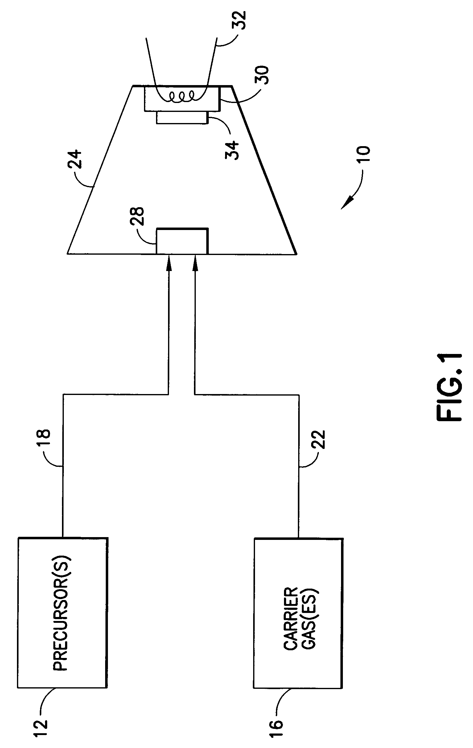
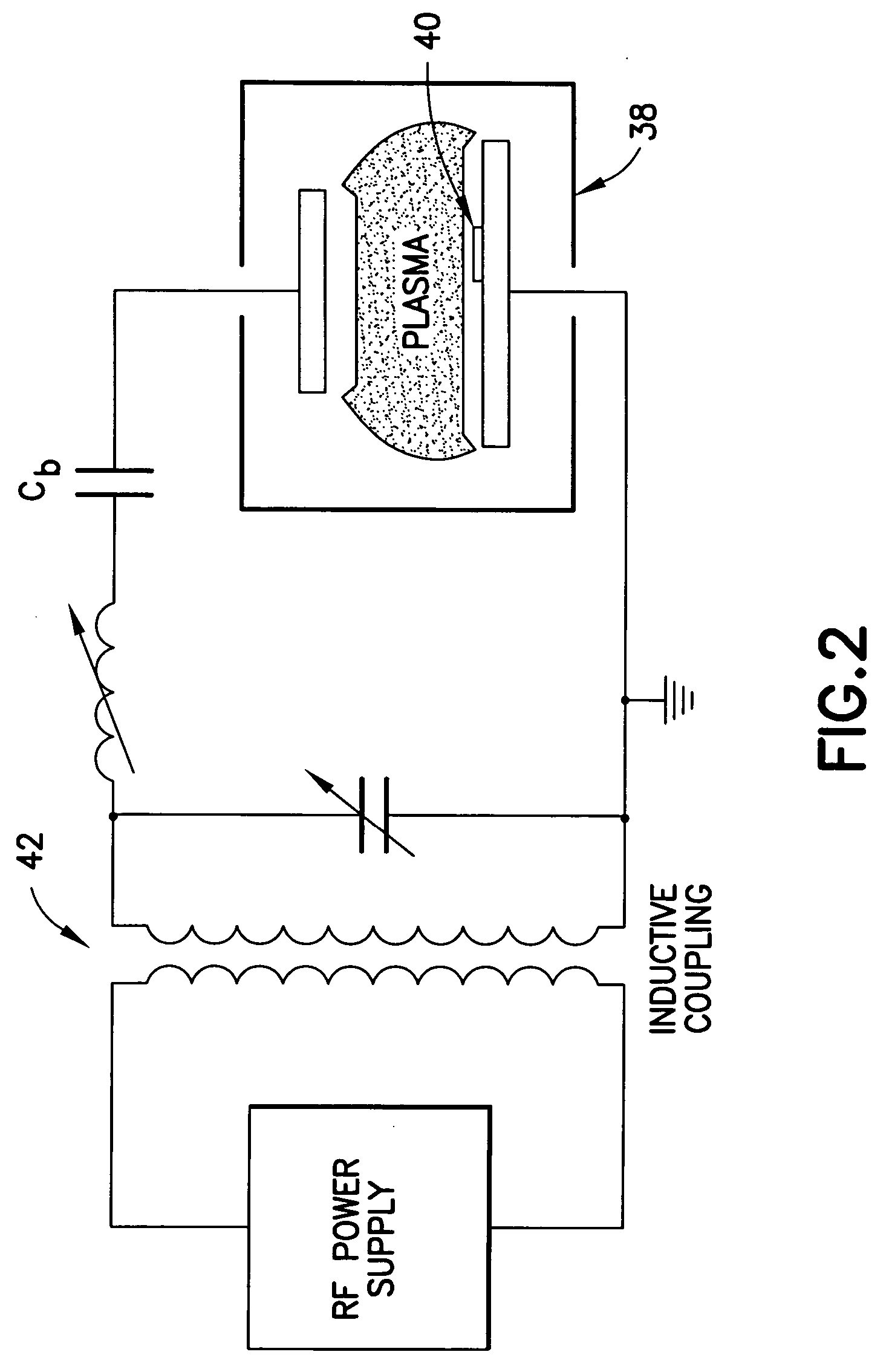
Image

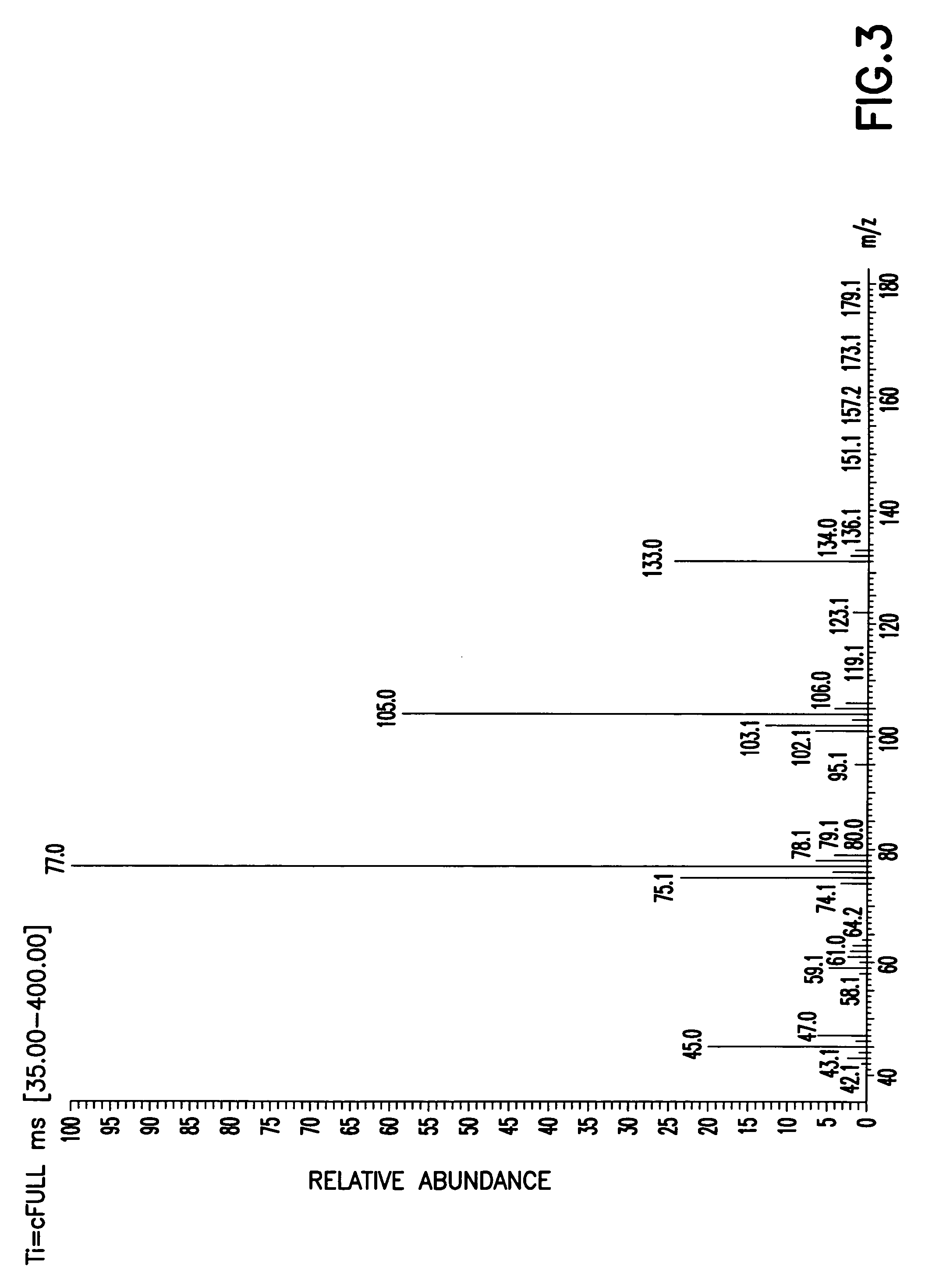
Examples
embodiment 1
In one embodiment (hereafter referred to as Embodiment 1) the invention relates to organosilicon precursors for producing porous, low dielectric constant, SiOC thin films, wherein the composition of the organosilicon precursor comprises at least one cleavable organic group that upon activation, rearranges, decomposes and / or cleaves as a highly volatile liquid or gaseous by product.
embodiment 2
In a further embodiment (hereafter referred to as Embodiment 2) the invention relates to organosilicon precursors useful for producing porous, low dielectric constant, SiOC thin films, comprising the general formula:
wherein R1 is a cleavable organic functional group, selected from the group consisting of C2 to C6 alkene, C2 to C6 alkyne, C3 to C4 allyl, C1 to C6 alkyl, C1 to C6 perfluoroalkyl; ligand X as described hereinbelow, and ligand Y as described hereinbelow; and each of R2 is same or different and each of R2 is selected from the group consisting of H, ligand X as described hereinbelow, ligand Y as described hereinbelow, C2 to C6 alkene, C2 to C6 alkyne, C3 to C4 allyl, C1 to C6 alkyl, C1 to C6 perfluoroalkyl, C1 to C6 alkoxy, aryl, perfluoroaryl and C2 to C6 alkylsilane; and
wherein R1 is a cleavable organic functional group, selected from the group consisting of C2 to C6 alkene, C2 to C6 alkyne, C3 to C4 allyl, C1 to C6 alkyl, C1 to C6 perfluoroalkyl; ligand X as desc...
embodiment 3
In a further embodiment (hereafter referred to as Embodiment 3) the invention relates to organosilicon precursors useful for producing porous, low dielectric constant, SiOC thin films, wherein the organosilicon precursor comprises a composition containing at least one alkyl group and at least one organic functional group that upon activation, rearranges, decomposes and / or cleaves as a highly volatile liquid or gaseous by product.
PUM
| Property | Measurement | Unit |
|---|---|---|
| Dielectric polarization enthalpy | aaaaa | aaaaa |
| Dielectric constant | aaaaa | aaaaa |
Abstract
Description
Claims
Application Information
 - Generate Ideas
- Intellectual Property
- Life Sciences
- Materials
- Tech Scout
- Unparalleled Data Quality
- Higher Quality Content
- 60% Fewer Hallucinations
Browse by: Latest US Patents, China's latest patents, Technical Efficacy Thesaurus, Application Domain, Technology Topic, Popular Technical Reports.
© 2025 PatSnap. All rights reserved.Legal|Privacy policy|Modern Slavery Act Transparency Statement|Sitemap|About US| Contact US: help@patsnap.com