Crystallization apparatus, crystallization method, method of manufacturing thin film transistor, thin film transistor, and display apparatus
- Summary
- Abstract
- Description
- Claims
- Application Information
AI Technical Summary
Benefits of technology
Problems solved by technology
Method used
Image

Examples
first application example of first embodiment
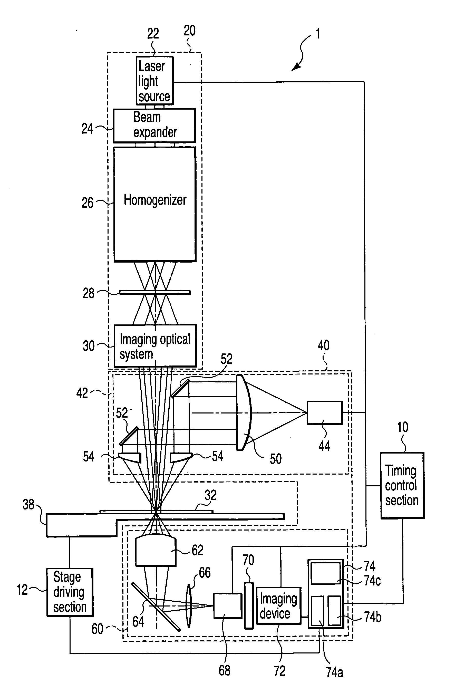
[0084] An example of application of the result of the observation of a crystallization process is the correction of a misalignment of the substrate 32 surface to a level of an imaging position of the imaging optical system 30. The misalignment of the level of the imaging position occurs for several reasons to be described below. When the surface of the substrate 32 is not aligned with the position at the imaging position of the crystallizing laser light, i.e., excimer laser light, the laser light intensity of the phase reversed part cannot be sufficiently reduced. Thus, the temperature of the phase reversed part after melting is higher than in the case in which the substrate 32 is at the imaging position. This causes a delay in the formation of a crystal nucleus and thus the start of crystallization delays. In addition, the crystal nucleus is created not only in the laser light phase reversed part but also in other parts randomly. Thus, growing crystal grains often collide against o...
second application example of first embodiment
[0088] Another example of application is to correct the misalignment of the in-plane position, that is, X-Y position of the substrate 32, using the laser crystallization apparatus 1 according to the present embodiment for observing a two-dimensional image of an area irradiated with an excimer laser light. The method of crystallization using a excimer laser light having an inverse-peak-like light intensity distribution formed by a phase shifter 28 is characterized in that the position at which crystal grains are formed can be predicted. For this observation, the microscopic observing optical system or monitoring section 60 is placed so that the photo detector 68 and the image intensifier 70 or only the photo detector 68 are / is temporarily withdrawn from the optical path of the imaging lens 66, while the imaging device 72 or the image intensifier 70 is moved to the position at an imaging position of the imaging lens 66. Thus, a two-dimensional image of the area in the crystallization ...
first embodiment
VARIATION OF FIRST EMBODIMENT
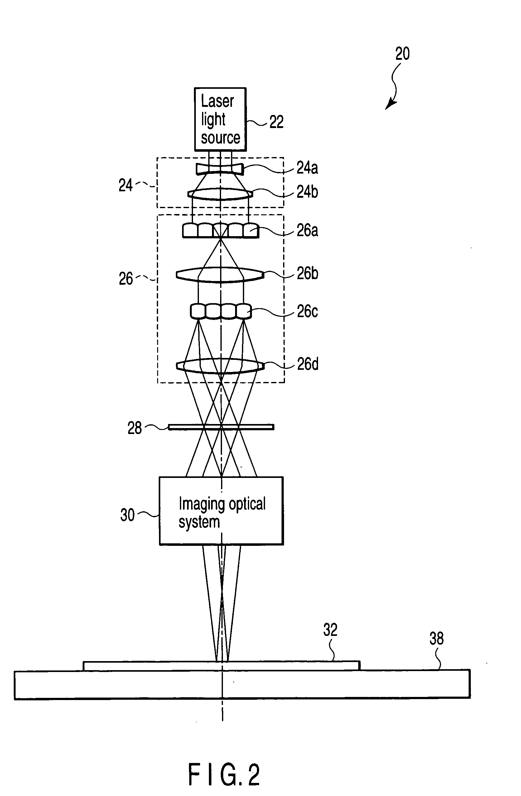
[0091]FIG. 10 shows a variation in the configuration of the first embodiment. In this variation, the phase shifter 28 and the imaging optical system 30 are removed from the configuration shown in FIG. 1, with the substrate 32 placed at a imaging position of a homegenizer 26. The present variation can reduce the number of optical elements such as lenses compared to the embodiment shown in FIG. 1. It is thus possible to apply a crystallizing laser light of an increased intensity.
[0092] The microscopic observing optical system or monitoring section 60 may not only be configured as previously described but may also be partly omitted or configured differently from the previously described one.
[0093] In a variation of the microscopic observing optical system or monitoring section 60, so called a gated CCD imaging device 73 can be used by omitting the streak tube 68, as shown in FIG. 11, the gated CCD imaging device 73 has a combined function with a image int...
PUM
| Property | Measurement | Unit |
|---|---|---|
| Area | aaaaa | aaaaa |
| Transparency | aaaaa | aaaaa |
| Energy | aaaaa | aaaaa |
Abstract
Description
Claims
Application Information
 - R&D Engineer
- R&D Manager
- IP Professional
- Industry Leading Data Capabilities
- Powerful AI technology
- Patent DNA Extraction
Browse by: Latest US Patents, China's latest patents, Technical Efficacy Thesaurus, Application Domain, Technology Topic.
© 2024 PatSnap. All rights reserved.Legal|Privacy policy|Modern Slavery Act Transparency Statement|Sitemap