Light generating semiconductor device and method of making the same

a semiconductor and light-generating technology, applied in semiconductor/solid-state device manufacturing, semiconductor devices, electrical equipment, etc., can solve the problems of reducing the efficiency of light generation in these semiconductor light-generating devices, and devices that do not provide desired light-emitting characteristics, so as to reduce the efficiency of light generation and high density of threading dislocations in the active layer

Inactive Publication Date: 2005-02-24
SUMITOMO ELECTRIC IND LTD
View PDF4 Cites 38 Cited by
  • Summary
  • Abstract
  • Description
  • Claims
  • Application Information

AI Technical Summary

Benefits of technology

[0005] The present inventors have found a technical problem on semiconductor light generating devices, such as the light emitting diode (LED). Since the semiconductor light generating devices use a sapphire substrate for making the above semiconductor structure for LEDs, the density of threading dislocations in the active layer is high. The semiconductor light generating device in the Publication 1 has the density of threading dislocations, 1.0×10⁹ per square centimeters (cm−2), and the semiconductor light generating device in the Publication 2 has a relatively low density of threading dislocations, 1.0×10⁷ per square centimeters (cm−2) The threading dislocations reduce the efficiency of light generation in these semiconductor light generating devices.

Problems solved by technology

The semiconductor light generating device in the Publication 1 has the density of threading dislocations, 1.0×10⁹ per square centimeters (cm−2), and the semiconductor light generating device in the Publication 2 has a relatively low density of threading dislocations, 1.0×10⁷ per square centimeters (cm−2) The threading dislocations reduce the efficiency of light generation in these semiconductor light generating devices.
Since the efficiency of light generation in the AlGaN light emitting devices is sensitive to threading dislocations in the active layers and the density of threading dislocations in AlGaN semiconductor light generating devices using sapphire substrate is high, these devices do not provide desired light emitting characteristics.

Method used


Image

  • Light generating semiconductor device and method of making the same
  • Light generating semiconductor device and method of making the same
  • Light generating semiconductor device and method of making the same

Examples


first embodiment

[0049] (First Embodiment)

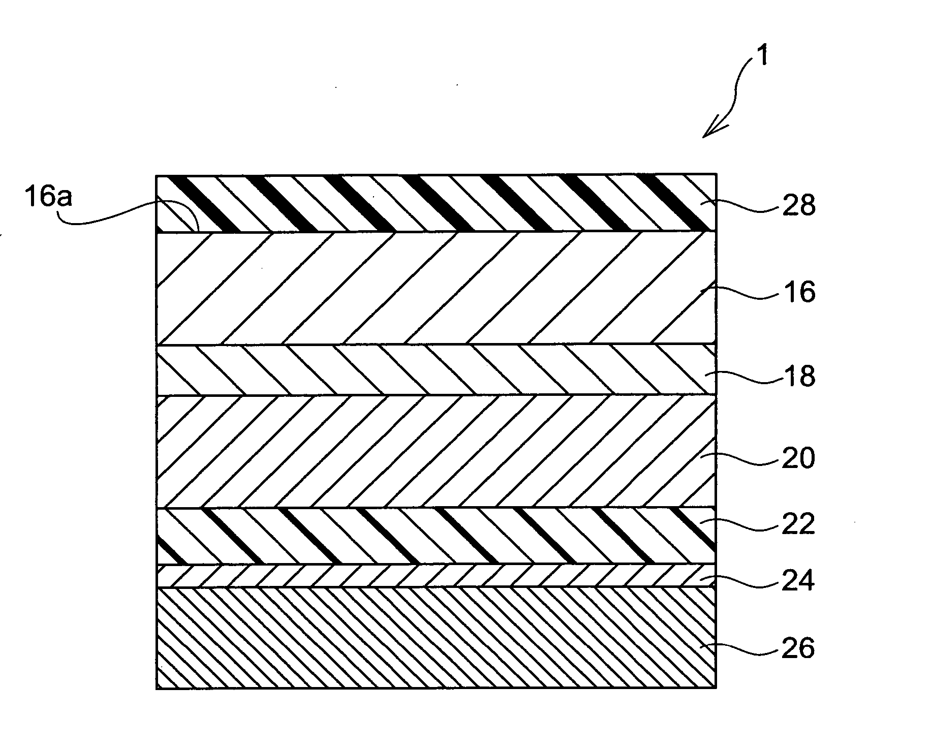
[0050] With reference to FIGS. 1 to 5, a semiconductor light generating device, such as a semiconductor light emitting diode 1, and a method of making the same according to the first embodiment of the present invention will be described.

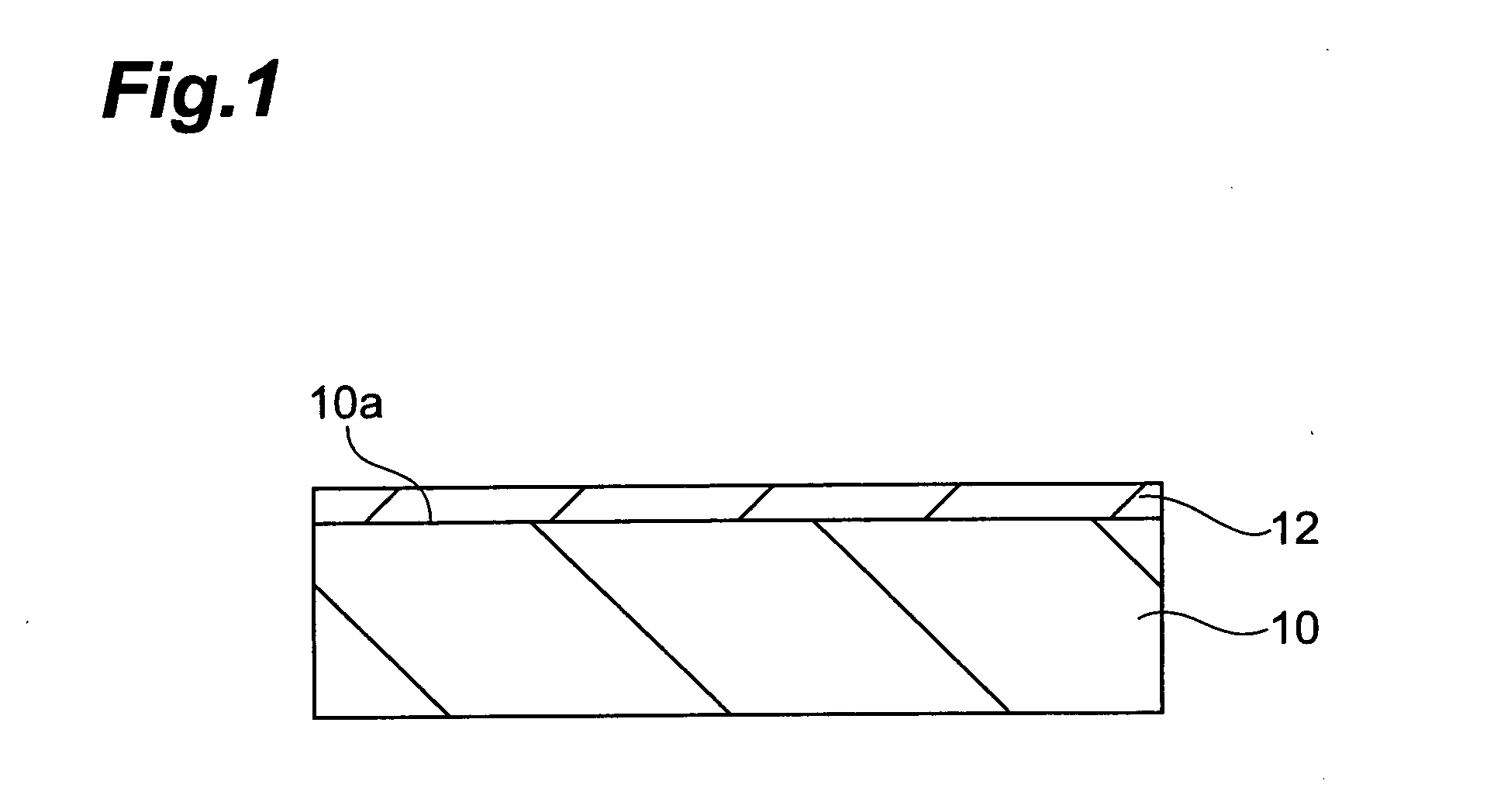
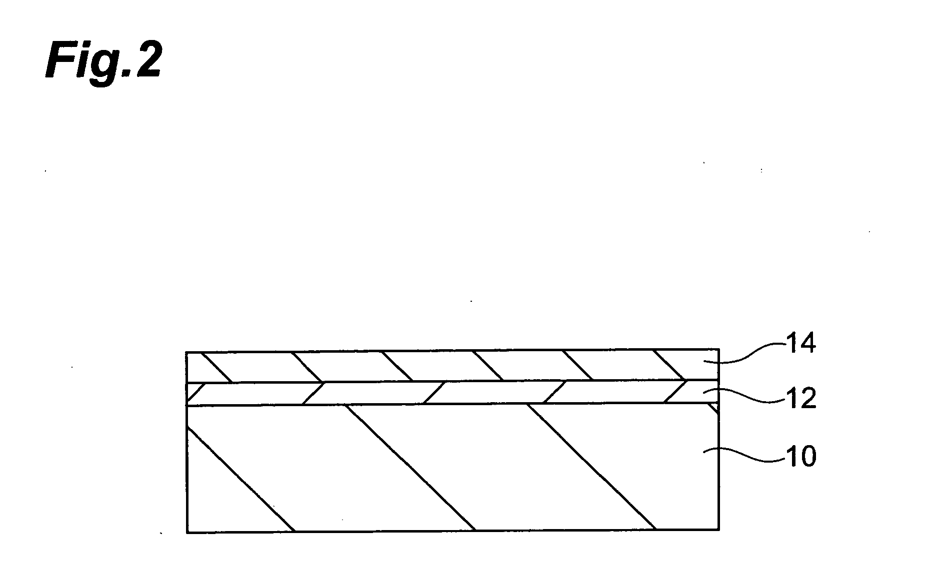
[0051] Referring to FIG. 1, a GaN substrate 10 is prepared. For example, the GaN substrate 10 may be made of GaN single crystal. The GaN substrate 10 is placed in the MOCVD apparatus (not shown) and the temperature of the GaN substrate 10 is increased to a temperature of 1050 degrees Celsius to carry out the thermal cleaning of the surface 10a of the GaN substrate 10. The thermal cleaning removes contaminants on the surface 10a and improves the evenness of the surface 10a. After the thermal cleaning, a gas including trimethylgallium (TMG) of a III group element source, ammonia (NH3) of a V group element source and silane (SiH4) of a doping element source are supplied to the MOCVD apparatus to form an n-type GaN buffer layer ...

second embodiment

[0067] (Second Embodiment)

[0068] With reference to FIGS. 7 to 12, a method of making a semiconductor light generating device 1A according to the second embodiment of the present invention will be described below.

[0069] A substrate 10A of single crystal AlVGa1-VN (010A is 0.18. The AlVGa1-VN substrate 10A is placed in an MOCVD apparatus to perform the thermal cleaning process of the AlVGa1-VN substrate 10A as is the GaN substrate in the first embodiment. For example, the temperature of the thermal cleaning process is 1050 degrees Celsius. At the same temperature as the thermal cleaning process, a gas including TMA and TMG of III group element sources, NH3 of a V group element source and SiH4 of a doping element source are supplied to the MOCVD apparatus to form an n-type AlWGa1-WN buffer layer 12A (010a of the AlVGa1-VN substrate 10A, as shown in FIG. 7. For example, the epitaxial growth temperature is 1050 degrees Celsius. For example, the composition W of the AlWGa1-WN buffer laye...


PUM


Abstract

In a method of making a semiconductor light generating device, a GaN-based semiconductor portion is formed on a GaN or AlGaN substrate. The GaN-based semiconductor portion includes a light generating film. An electrode film is formed on the GaN-based semiconductor film. A conductive substrate is bonded to a surface of the electrode film using a conductive adhesive. After bonding the conductive substrate, the GaN or AlGaN substrate is separated from the GaN-based semiconductor portion to form the semiconductor light generating device.

Description

BACKGROUND OF THE INVENTION [0001] 1. Field of the Invention [0002] This invention relates to a semiconductor light generating device for the generation of ultraviolet light and so on, and relates to a method of making the ultraviolet light generating semiconductor device. [0003] 2. Related Background Art [0004] Publication 1 (Jpn. J. Appl. Phys. Vol. 41 pp. L1434-1436) and Publication 2 (50th Conference of Japan Society of Applied Physics, Extended Abstract, pp. 431) disclose semiconductor light generating devices. These semiconductor light generating devices include a Cu—W substrate and a semiconductor structure for light emitting diodes (LEDs). This light emitting diode semiconductor structure has an active layer of an InGaN multiple quantum structure. A Au—Sn layer is formed on the Cu—W substrate. The active layer in the light emitting diode semiconductor structure is provided between a p-electrode for p-type semiconductor and an n-electrode for n-type semiconductor. The semicon...

Claims


Application Information

Patent Timeline
Patent Type & Authority Applications(United States)
IPC IPC(8): H01L33/32H01L21/00H01L33/40
CPCH01L33/0079H01L33/0075H01L33/0093Y10S438/977
Inventor AKITA, KATSUSHI
Owner SUMITOMO ELECTRIC IND LTD
Why Eureka
Try Eureka