Illumination system with spatially controllable partial coherence compensating for line width variances

a partial coherence and line width technology, applied in the field of semiconductor manufacturing, can solve the problems of not optimizing images, unable to provide images of reticles onto photosensitive substrates, etc., and achieve the effects of improving imaging, improving photolithographic tools or systems, and easy chang

Inactive Publication Date: 2005-02-24
ASML HLDG NV
View PDF27 Cites 5 Cited by
  • Summary
  • Abstract
  • Description
  • Claims
  • Application Information

AI Technical Summary

Benefits of technology

It is an advantage of the present invention that the illumination system can easily be changed to improve imaging or adapt to changes in the projection optics.
It is a feature of the present invention that different illumination regions of an optical element are used to locally modify illumination of a reticle and improve performance of the photolithographic tool or system.
It is another feature of the present invention tha...

Problems solved by technology

However, due to the complexity of illumination sources and the difficulty of modifying them for a particular optical system to compensate for variations of the photolithographic system, and in particular the projection optics, often the image is not optimize...

Method used


Image

  • Illumination system with spatially controllable partial coherence compensating for line width variances
  • Illumination system with spatially controllable partial coherence compensating for line width variances
  • Illumination system with spatially controllable partial coherence compensating for line width variances

Examples


Embodiment Construction

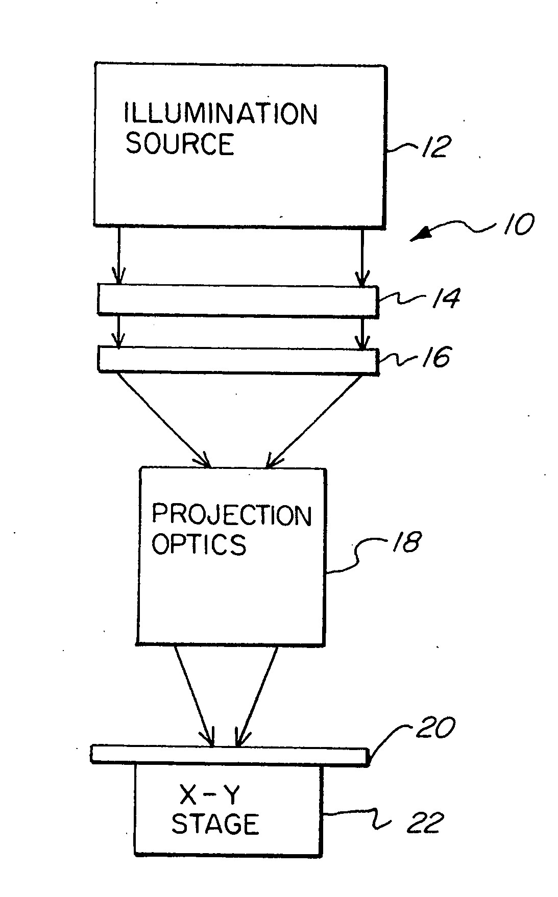
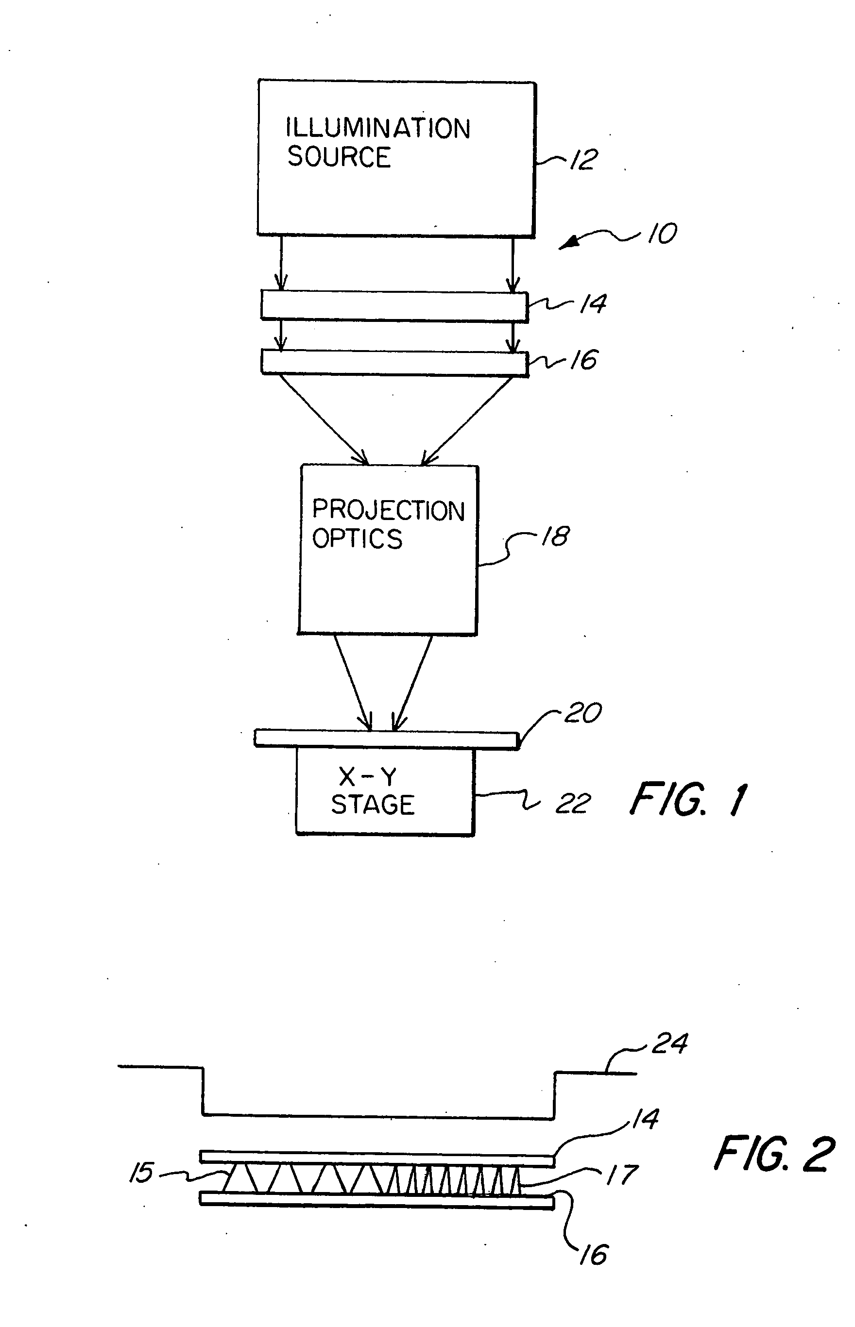
FIG. 1 schematically illustrates a photolithographic system 10. Illumination source 12 projects electromagnetic radiation through an optical element 14 and onto a reticle 16. An illumination plane is formed at the reticle 16. An image of the reticle 16 is projected onto a wafer 20 by projection optics 18. Wafer 20 has a photosensitive resist coating thereon which is exposed by the image of the reticle 16. Wafer 20 is mounted on a wafer stage 22 which is movable in the X and Y direction. In some photolithography operations, the wafer stage 22 may also be scanned along one axis. The illumination source 12 may be any illumination source or system, such as that disclosed in U.S. Pat. No. 5,631,721, entitled “Hybrid Illumination System For Use In Photolithography” by Stanton et al, which is herein incorporated by reference in its entirety.

FIG. 2 illustrates an illumination profile 24 created by the illumination source 12, illustrated in FIG. 1. Generally, it is desirable that the intensi...


PUM


Abstract

An illumination system having an array optical element with different illumination regions corresponding or matched to different line width variations printed on a photosensitive material. The array optical element may be a filter, diffractive optical element, or micro lens array having illumination regions producing different types of illumination properties or characteristics. Each of the illumination regions are matched or correspond to a respective region on a patterning device to provide optimized exposure of a photosensitive material. The optical element may be used to tailor a conventional illumination system to the unique characteristics of the projection optics used in a system, thereby compensating for vertical and horizontal bias or variations in line width for features oriented in the vertical and horizontal direction.

Description

FIELD OF THE INVENTION The present invention relates generally to semiconductor manufacturing, and more particularly to an illumination system that is locally spatially controllable to reduce line width variations in a lithographic system. BACKGROUND OF THE INVENTION Photolithography is often used in the manufacture of semiconductors. The image of a reticle having a circuit pattern thereon is projected onto a photosensitive substrate such as a wafer. The wafer is subsequently processed, forming printed patterns thereon. This process is generally repeated several times, forming multiple layers. As the art develops and the element sizes of the semiconductor devices become smaller, there is a need for improved illumination sources used in the lithographic printing systems. Accordingly, there have been many types of illumination systems disclosed which may enhance the quality of imaging of a reticle onto a photosensitive substrate. One such illumination system is disclosed in U.S. Pat...

Claims


Application Information

Patent Timeline
IPC IPC(8): G02B5/18G02B3/00G02B3/04G02B19/00G03F7/20H01L21/027
CPCG03F7/70125H01L21/027
Inventor MCCULLOUGH, ANDREW W.GALLATIN, GREGG M.
Owner ASML HLDG NV
Why Eureka
Try Eureka