Integrated circuit identification

a technology of integrated circuits and integrated circuits, applied in semiconductor/solid-state device testing/measurement, printing, instruments, etc., can solve the problems of complicated marking task, limited traceability of particular chips, and high cost of spa

Inactive Publication Date: 2005-02-24
TEXAS INSTR INC
View PDF3 Cites 24 Cited by
  • Summary
  • Abstract
  • Description
  • Claims
  • Application Information

AI Technical Summary

Benefits of technology

[0007] An advantage of the invention is that it allows for a chip-level custom identification mark for each chip on a wafer.
[0008] The invention can be more fully understood by reading the following detailed description of preferred embodiments of the invention with reference to the accompanying drawings. One skilled in the art will appreciate that the drawings are not to sc

Problems solved by technology

Since, for a given level in the fabrication of the chip, that same reticle is stepped across the entire wafer, it has not been possible to give each individual chip its own identifying mark during the wafer fabrication process, where it is most cost efficient to do so.
Thus, a problem with a particular chip can only also be traced back as far as the level of identificati

Method used


Image

  • Integrated circuit identification
  • Integrated circuit identification
  • Integrated circuit identification

Examples


Embodiment Construction

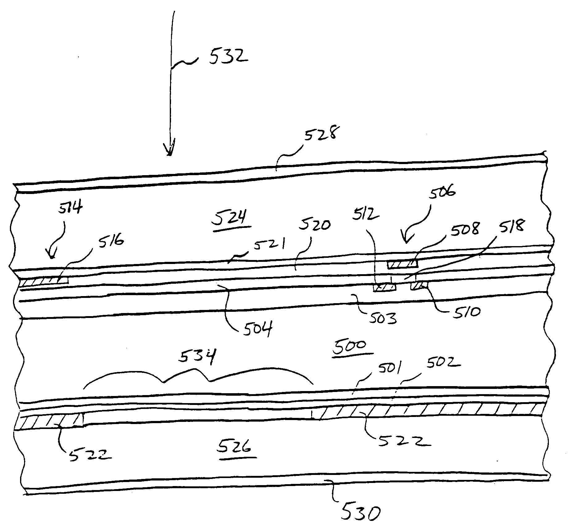
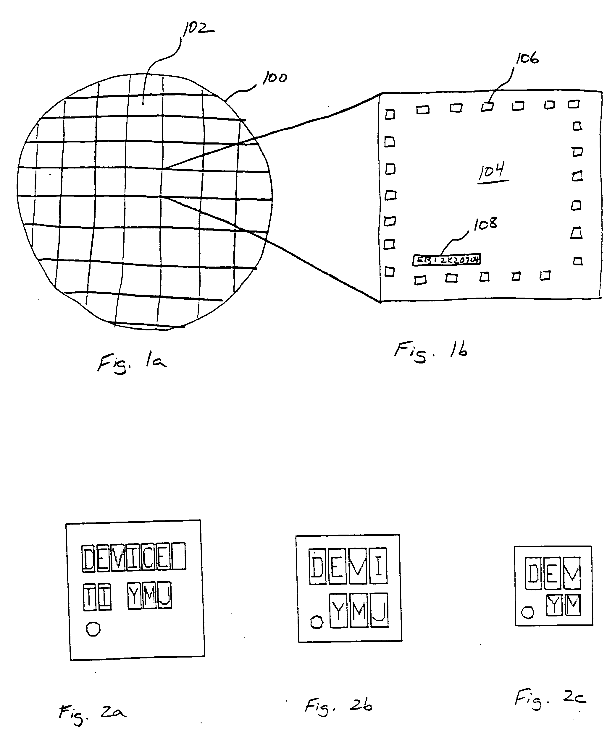
[0019]FIG. 1a shows a plan view of a wafer 100 segmented into individual dice or chips 102. FIG. 1b shows detail of a particular chip 104, including bond pads 106, and an identifying mark 108. Ideally, the mark would contain information indicating the facility in which the chip was made, the day, month, and year on which it was made, the lot of wafers with which it was processed, as well as the number of the wafer in that lot, and, finally, the location the particular die occupies upon the wafer. Such a mark may appear as follows: “EBT2K20704-MIB-02-17,” where “EBT” is the fabrication facility, “2K2” is 2002, the year of fabrication, “07” is July, the month of fabrication, “04” is the fourth day of July, “MIB” is the lot identifier, “02” is the wafer number within the lot, and “17” is the die location on the wafer. Of course, a manufacturer ID also appears at some location on the chip. Putting this much information on a chip in a conventional size and lettering format can consume to...


PUM


Abstract

A method for marking a semiconductor wafer 302 includes the steps of: providing a reticle 300 including liquid crystal pixels; positioning the semiconductor wafer in proximity to the reticle; directing radiation through a first plurality of the pixels onto a first location on the wafer; changing the relative positions of the semiconductor wafer and the reticle; and directing radiation through a second plurality of the pixels onto a second location on the wafer. The first plurality of pixels can be used to form a first mark and the second plurality of pixels can be used to form a second mark, wherein the second mark is different from the first mark. The marks can be made of a pattern of dots in order to save space. The pixels can be selected to form certain marks by using a computer 304 to turn on or off a transistor that may be associated with each pixel. Also described is a system for marking a semiconductor wafer. The system includes a wafer mount 301; a radiation source 306 in proximity to the wafer mount; a reticle 300 which includes liquid crystal pixels and that is positionable between the radiation source and the wafer mount; and a mechanism 303 for changing the relative positions of the reticle and the wafer mount. The radiation source can be non-coherent far-ultraviolet, near-ultraviolet, or visible sources, or a laser.

Description

BACKGROUND OF THE INVENTION [0001] This invention is in the field of integrated circuits and in the field of marking integrated circuits for tracking purposes. [0002] There is a need in the semiconductor industry for a reliable method of marking integrated circuit die (“chips”) to facilitate tracking of these devices after they are manufactured and sent to customers worldwide. For example, in instances where a customer detects an imperfection in a particular chip, or desires more chips that behave like a particular chip, the ability to ascertain the provenance of the chip and the conditions under which it was fabricated can constitute a competitive advantage for an integrated circuit manufacturer. Whereas, in the past, the marking of the chips on a particular wafer has been possible, it has been possible to only mark chips with a gross level of identification, since all of the chips on a wafer in a given lot of wafers of a particular type of integrated circuit are made with the same...

Claims


Application Information

Patent Timeline
IPC IPC(8): G03F1/00G03F1/38G03F7/20H01L21/02H01L21/027H01L23/544
CPCG03F1/14G03F1/38G03F7/2057G03F7/70291G03F7/70383G03F7/70541H01L23/544H01L2924/0002H01L2223/54406H01L2223/54433H01L2223/54473H01L2223/5448H01L2924/00H01L21/02G01R31/26G01N21/86
Inventor MATSUNAMI, AKIRA
Owner TEXAS INSTR INC
Why Eureka
Try Eureka