Thin-film field effect transistor and making method

a technology of field effect transistor and thin film, which is applied in the direction of transistors, solid-state devices, thermoelectric devices, etc., can solve the problems of imposing a certain limit in reducing the cost of tft manufacture, causing slight defects, and ordinary metal-based semiconductors used in the art cannot avoid the problem, etc., to achieve greater carrier mobility, minimize defects, and reduce the effect of manufacturing cos

Inactive Publication Date: 2005-03-03
SHIN ETSU CHEM IND CO LTD
View PDF8 Cites 13 Cited by
  • Summary
  • Abstract
  • Description
  • Claims
  • Application Information

AI Technical Summary

Benefits of technology

[0007] An object of the present invention is to provide thin-film field effect transistors (TFTs) having a higher carrier mobility than prior art TFTs and minimized defects, and a method of fabricating the same.
[0008] The inventor has discovered that in a TFT with a metal-insulator-semiconductor (MIS) structure, a simple approach of using organic solvent-soluble polymers as the materials of which the semiconductor and insulating layers are made is successful in achieving a greater carrier mobility than in the prior art.
[0009] Accordingly, the present invention provides a thin-film field effect transistor with an MIS structure, wherein the materials of which the semiconductor and insulating layers are made are polymers which are dissolvable in organic solvents and have a weight average molecular weight of more than 2,000 to 1,000,000.
[0010] In another embodiment of the invention, a thin-film field effect transistor is fabricated by a process involving the steps of dissolving polymers having a weight average molecular weight (Mw) of more than 2,000 to 1,000,000 in organic solvents, applying the resulting polymer solutions, and drying the applied polymer solutions, thereby forming a semiconductor layer and an insulating layer.
[0011] According to the invention, use of polymers for both the semiconductor layer and insulating layer of TFT eliminates such treatments as patterning and etching using photoresists or the like in the circuit forming technology using prior art metal based semiconductors and insulators, reduces the probability of TFT defects and achieves a reduction of TFT manufacture cost.

Problems solved by technology

However, ordinary metal based semiconductors used in the art cannot avoid the problem that slight defective pixels are caused by the defects of TFTs formed on the substrate as a result of treatments including patterning and etching using photoresists during circuitry formation on the substrate.
Such treatments impose a certain limit in reducing the cost of TFT manufacture.
The recent trend toward larger size and more precise definition tends to increase the probability of defection in the TFT manufacture.
Since the semiconductor layer is formed by evaporating α-sexithienyl as an organic semiconductor material, treatments including patterning and etching using photoresists are necessary, failing to achieve a cost reduction.

Method used


Image

  • Thin-film field effect transistor and making method
  • Thin-film field effect transistor and making method

Examples


example 1

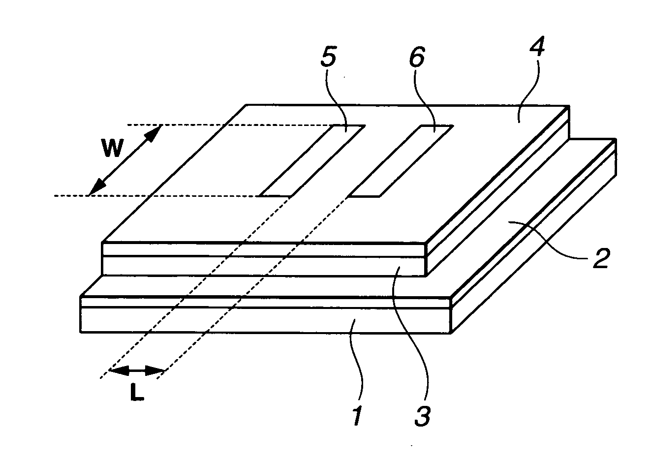
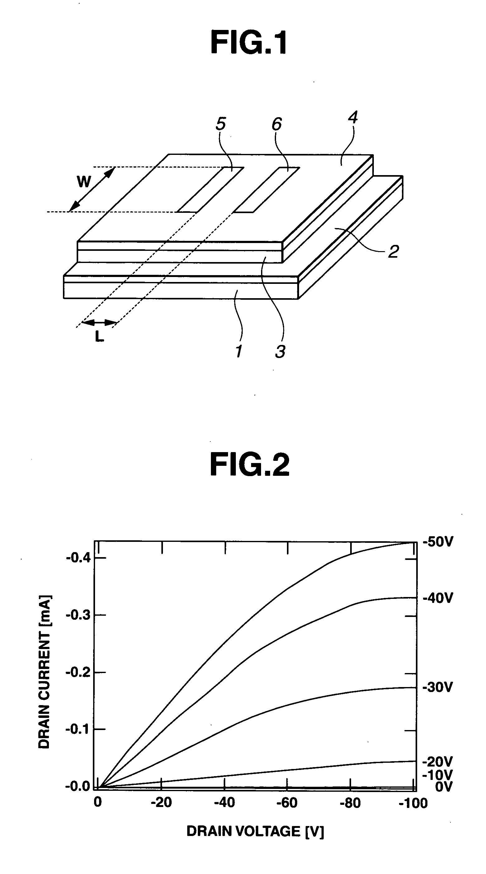
[0027] There were furnished cyanoethyl pullulan having a substitution of cyanoethyl of 85.2 mol % (CyEPL, Shin-Etsu Chemical Co., Ltd., CR-S, Mw=49,000) as an insulating layer material and poly(3-hexylthiophene) (P3HT, Aldrich, Mw=87,000) as an organic semiconductor layer material. The organic solvent in which P3HT was dissolved was chloroform, in which CyEPL was insoluble. A TFT was fabricated using these materials and evaluated as follows.

[0028] On a glass (SiO2) substrate, a gate electrode was formed by depositing Ti to a thickness of 5 nm and then Au to a thickness of 20 nm, using an RF sputtering technique at room temperature and a back pressure of 10−4 Pa.

[0029] An insulating layer was then formed on the gate electrode by dissolving 15 wt % CyEPL as the insulating layer material in N-methyl-2-pyrrolidone, passing the solution through a 0.2-micron membrane filter, spin coating the solution, and drying at 100° C. for one hour.

[0030] A semiconductor layer of 50 nm thick was th...


PUM

PropertyMeasurementUnit
dielectric constantaaaaaaaaaa
thicknessaaaaaaaaaa
thicknessaaaaaaaaaa

Abstract

In a thin-film field effect transistor with a MIS structure, the materials of which the semiconductor and insulating layers are made are polymers which are dissolvable in organic solvents and have a weight average molecular weight of more than 2,000 to 1,000,000. Use of polymers for both the semiconductor layer and insulating layer of TFT eliminates such treatments as patterning and etching using photoresists in the prior art circuit-forming technology, reduces the probability of TFT defects and achieves a reduction of TFT manufacture cost.

Description

CROSS-REFERENCE TO RELATED APPLICATION [0001] This Nonprovisional application claims priority under 35 U.S.C. §119(a) on Patent Application No. 2003-304019 filed in Japan on Aug. 28, 2003, the entire contents of which are hereby incorporated by reference. TECHNICAL FIELD [0002] This invention relates to thin-film field effect transistors (TFTs) utilizing silicon semiconductors or compound semiconductors, especially for use in liquid crystal displays, and a method of fabricating the same. BACKGROUND ART [0003] TFTs utilizing silicon semiconductors or compound semiconductors are used in common integrated circuits and in wide-spreading other applications. In particular, the use of TFTs in liquid crystal displays is well known. Nowadays LC displays are making continuous progress toward larger size and more precise definition. The requirement to incorporate a greater number of TFTs corresponding to the number of pixels becomes stronger than ever. [0004] However, ordinary metal based semi...

Claims


Application Information

Patent Timeline
Patent Type & Authority Applications(United States)
IPC IPC(8): H01L21/335H01L29/772H01L51/05H01L29/786H01L35/24H01L51/00H01L51/30H01L51/40
CPCH01L51/0007H01L51/0558H01L51/052H01L51/0036H10K71/15H10K85/113H10K10/471H10K10/484H01L29/772
Inventor FUKUI, IKUO
Owner SHIN ETSU CHEM IND CO LTD
Why Eureka
Try Eureka