Semiconductor device and method of manufacturing the same

a semiconductor and semiconductor technology, applied in semiconductor devices, diodes, electrical devices, etc., can solve the problems of deteriorating the surface of silicon carbide substrates, affecting the performance of the related art, so as to reduce the concentration of impurities, increase the withstand voltage, and increase the leakage current

Active Publication Date: 2005-03-03
NISSAN MOTOR CO LTD
View PDF6 Cites 61 Cited by
  • Summary
  • Abstract
  • Description
  • Claims
  • Application Information

AI Technical Summary

Benefits of technology

[0005] The related art may reduce an impurity concentration in the electric field relaxation region, to increase a withstand voltage between the epitaxial region and the electric field relaxation region. This, however, expands a depletion layer into the whole of the electric field relaxation region, to expose an end of the heterojunction to an electric field spread in the epitaxial region. This results in increasing a leakage current at the end of the heterojunction. Namely, according to the related art, the effect of increasing the withstand voltage of the epitaxial region with the use of the electric field relaxation region conflicts with the effect of preventing a leakage current occurring at an end of the polysilicon region.

Problems solved by technology

Namely, it is difficult for the related art to achieve a high disconnection performance and a high temperature characteristic superior to those of the Schottky junction.
This results in increasing a leakage current at the end of the heterojunction.
Such a high-temperature heat treatment deteriorates the surface of the silicon carbide substrate.
On the surface of such a deteriorated silicon carbide substrate, it is impossible to form a good Schottky junction that can provide a diode having a high withstand voltage.

Method used


Image

  • Semiconductor device and method of manufacturing the same
  • Semiconductor device and method of manufacturing the same
  • Semiconductor device and method of manufacturing the same

Examples


first embodiment

[0044] (First Embodiment)

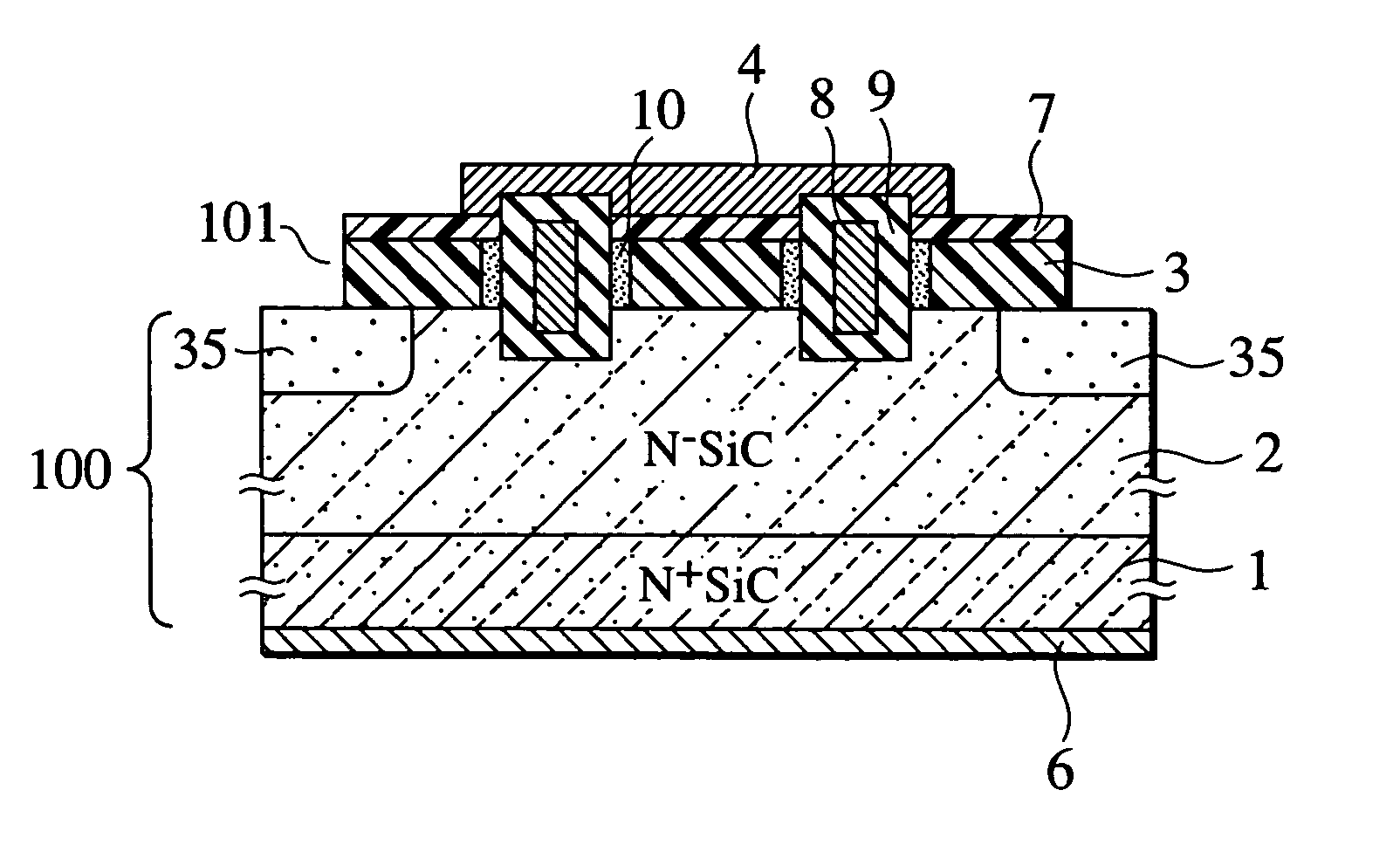
[0045]FIG. 1 is a sectional view showing a semiconductor device according to a first embodiment of the present invention. According to this embodiment, the semiconductor device employs a silicon carbide substrate 1. The silicon carbide substrate 1 is made of an n+-type and is made of, for example, silicon carbide of polytype 4H. On the substrate 1, an n−-type epitaxial region 2 is formed to provide a silicon carbide semiconductor base 100. The substrate 1 has, for example, a specific resistance of several mΩ (milliohm(s)) cm to several tens of Ω (ohm) cm and a thickness of about 200 to 400 μm (micro meter(s)). The epitaxial region 2 has, for example, an n-type impurity concentration of 1015 to 1018 cm−3 and a thickness of several μm (micro meter(s)) to several tens of μm (micro meter(s)). According to this embodiment, the epitaxial region 2 has an impurity concentration of 1016 cm−3 and a thickness of 10 μm (micro meter(s)). Although the first embodiment is ...

second embodiment

[0069] (Second Embodiment)

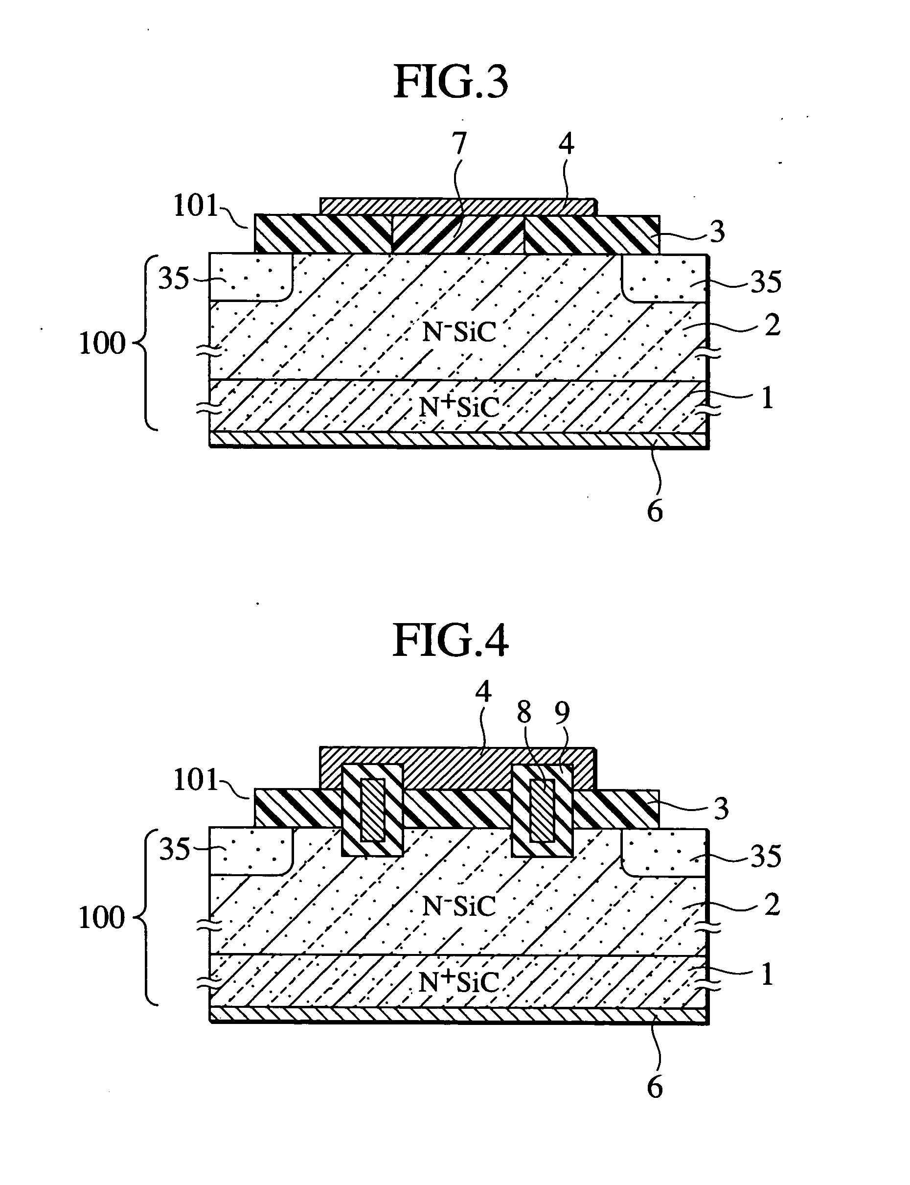
[0070]FIG. 4 is a sectional view showing a semiconductor device according to a second embodiment of the present invention and corresponding to the structure of the first embodiment shown in FIG. 2. Parts of the second embodiment that operate like those of FIG. 2 will not be explained and parts that are specific to the second embodiment will be explained in detail.

[0071] In FIG. 4, a part of a heterojunction interface of a heterojunction diode (FIG. 2) is provided with a gate electrode 8 covered with a gate insulating film 9, to form a transistor. In FIG. 4, the second embodiment forms trenches in an epitaxial region 2. It is also possible to employ a planar structure having no trenches.

[0072] Operation of the second embodiment will be explained. For example, a surface electrode 4 is grounded and a positive potential is applied to a bottom metal electrode 6. For example, a ground potential or a negative potential is applied to the gate electrode 8, to keep...

third embodiment

[0094] (Third Embodiment)

[0095]FIG. 14 is a sectional view showing a silicon carbide semiconductor device according to a third embodiment of the present invention. In FIG. 14, an n+-type silicon carbide substrate 1 and an n−-type epitaxial region 2 formed on the substrate 1 form an n-type silicon carbide semiconductor base 100. Here, the n-type is a first conductivity type and silicon carbide is a first semiconductor material.

[0096] On a first principal face of the silicon carbide semiconductor base 100, i.e., on the epitaxial region 2, an n-type polysilicon region 63A is formed. The n-type polysilicon that forms the region 63A has a different band gap from silicon carbide and serves as a second semiconductor material. Between the epitaxial region 2 and the polysilicon region 63A, a heterojunction is formed.

[0097] On the first principal face of the silicon carbide semiconductor base 100, i.e., on the epitaxial region 2, an electric field relaxation part 65 is formed to include an ...


PUM


Abstract

An aspect of the present invention provides a semiconductor device that includes a first semiconductor region of a first conductivity type and a second semiconductor region of a second conductivity type, having a different band gap from the first semiconductor region and forming a heterojunction with the first semiconductor region.

Description

BACKGROUND OF THE INVENTION [0001] The present invention relates to a semiconductor device and a method of manufacturing the same, and particularly, to a semiconductor device having a heterojunction and a method of manufacturing the same. [0002] Japanese Laid-Open Patent Publication No. 2003-318413 discloses a semiconductor device having a semiconductor base made of an n+-type silicon carbide substrate region and an n−-type epitaxial region formed on the substrate region. On one principal face of the semiconductor base, an n-type polysilicon region is formed. The epitaxial region and n-type polysilicon region form a heterojunction. In contact with an end of the heterojunction, a p-type electric field relaxation region is formed. On a bottom face of the n+-type silicon carbide substrate region, a bottom electrode is formed. On the surface of the polysilicon region, a surface electrode is formed. [0003] On the other hand, a Schottky junction is a junction that uses conventional silico...

Claims


Application Information

Patent Timeline
Patent Type & Authority Applications(United States)
IPC IPC(8): H01L21/04H01L29/24H01L29/739H01L29/78H01L29/808H01L29/861H01L29/872
CPCH01L21/046H01L29/1608H01L29/66068H01L29/7395H01L29/7802H01L29/165H01L29/7828H01L29/8083H01L29/861H01L29/872H01L29/7827H01L29/7805
Inventor HAYASHI, TETSUYATANAKA, HIDEAKIHOSHI, MASAKATSUKANEKO, SAICHIROU
Owner NISSAN MOTOR CO LTD
Why Eureka
Try Eureka