Single poly-emitter PNP using DWELL diffusion in a BiCMOS technology

a single-poly-emitter, dwell diffusion technology, applied in the direction of semiconductor devices, basic electric elements, electrical equipment, etc., can solve the problems of punch-through breakdown condition, transistor breakdown voltage may be an issue, performance trade-offs, etc., to facilitate the formation of a small emitter

Inactive Publication Date: 2005-03-03
TEXAS INSTR INC
View PDF7 Cites 12 Cited by
  • Summary
  • Abstract
  • Description
  • Claims
  • Application Information

AI Technical Summary

Benefits of technology

[0014] The present invention relates to a method of forming a bipolar transistor device, and more particularly a vertical poly-emitter PNP transistor, as part of a BiCMOS type manufacturing process. The formation of the PNP transistor during a CMOS / DMOS fabrication process relies on merely one additional mask that facilitates formation of a small emitter in a portion of an N-type surface layer of a double diffused DWELL. The DWELL includes a P-type body layer formed via implantation through the same opening in the same mask utilized to establish the N-type surface layer.

Problems solved by technology

While such integration does serve to minimize manufacturing costs, in some cases the integration causes performance tradeoffs to be made.
The NPN bipolar transistor 10 of prior art FIG. 1 may be employed in various types of applications, and in some applications the transistor breakdown voltage may be an issue.
The thin epi 16 in that region limits transistor BVCEO by letting the space charge region at the NBL and epi junction reach the emitter during device operation, disadvantageously resulting in a punch-through breakdown condition.
Such additional actions are disadvantageous when attempting to minimize costs in the fabrication process.
This is disadvantageous in transistor applications where a high gain is important or desired.
As such, devices produced thereby experience some of the aforementioned deficiencies.
Some vertical PNPs do exist, however, but these PNPs are substrate PNP devices which inject current into the substrate and cause undesirable substrate debiasing and latchup.
Lateral PNPs similarly have undesirable characteristics in that they are large and slow.
Moreover, conventional poly-emitter PNPs require two to four additional masks to be formed, thus adding expense to the manufacturing process.
Similarly, a poly-silicon-emitter PNP can be formed in a SiGe-base heterojunction bipolar transistor (HBT) process, but such a process is complex and expensive aiming at high performance.
Such a process is not, however, cost effective.

Method used


Image

  • Single poly-emitter PNP using DWELL diffusion in a BiCMOS technology
  • Single poly-emitter PNP using DWELL diffusion in a BiCMOS technology
  • Single poly-emitter PNP using DWELL diffusion in a BiCMOS technology

Examples


Embodiment Construction

[0022] One or more aspects of the present invention are described with reference to the drawings, wherein like reference numerals are generally utilized to refer to like elements throughout, and wherein the various structures are not necessarily drawn to scale. In the following description, for purposes of explanation, numerous specific details are set forth in order to provide a thorough understanding of one or more aspects of the present invention. It may be evident, however, to one skilled in the art that one or more aspects of the present invention may be practiced with a lesser degree of these specific details. In other instances, well-known structures and devices are shown in block diagram form in order to facilitate describing one or more aspects of the present invention.

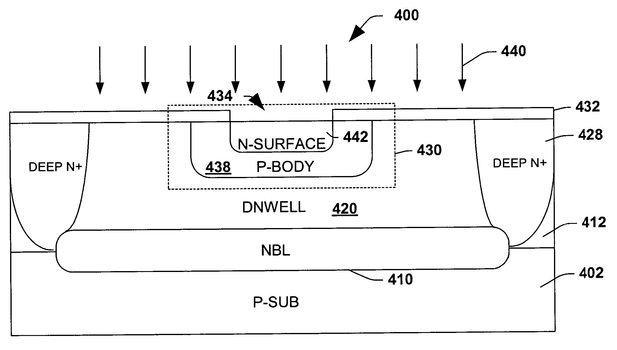
[0023] One or more aspects of the present invention pertain to a method of forming a bipolar transistor device, and more particularly a vertical poly-emitter PNP transistor, as part of a BiCMOS type manufact...


PUM


Abstract

A method of forming a bipolar transistor device, and more particularly a vertical poly-emitter PNP transistor, as part of a BiCMOS type manufacturing process is disclosed. The formation of the PNP transistor during a CMOS / DMOS fabrication process requires merely one additional mask to facilitate formation of a very small emitter in a portion of an N-type surface layer of a double diffused well (DWELL). Unlike conventional PNP transistors, a separate mask is not required to establish the base of the transistor as the transistor base is formed from a portion of the double diffused well and the DWELL includes a P-type body layer formed via implantation through the same opening in the same mask utilized to establish the N-type surface layer of the double diffused well. The base is also thin thus improving the transistor's frequency and gain.

Description

FIELD OF INVENTION [0001] The present invention relates generally to semiconductor devices and more particularly relates to a method of efficiently forming a poly-emitter bipolar transistor as part of a CMOS / DMOS fabrication process. BACKGROUND OF THE INVENTION [0002] Integrated circuits having bipolar and MOS transistors formed on the same semiconductor substrate have many uses in the electronics industry and are therefore in great demand. One significant advantage of such devices is that they combine the high power and fast switching speeds of bipolar devices with the high density and low power consumption of MOS transistors. The diversity of uses for such BiCMOS devices has fueled a surge toward fabricating faster, denser and more powerful integrated BiCMOS devices by more individual device enhancing manufacturing processes. [0003] When forming devices using a BiCMOS manufacturing process, care is taken to minimize the number of masks employed therein to lower the manufacturing c...

Claims


Application Information

Patent Timeline
Patent Type & Authority Applications(United States)
IPC IPC(8): H01L21/331H01L21/8249H01L29/08H01L29/735
CPCH01L21/8249H01L29/735H01L29/6625H01L29/0808
Inventor SPRINGER, LILY
Owner TEXAS INSTR INC
Why Eureka
Try Eureka