

Pfet-based ESD protection strategy for improved external latch-up robustness
- Summary
- Abstract
- Description
- Claims
- Application Information
AI Technical Summary
Benefits of technology
Problems solved by technology
Method used
Image

Examples
Embodiment Construction
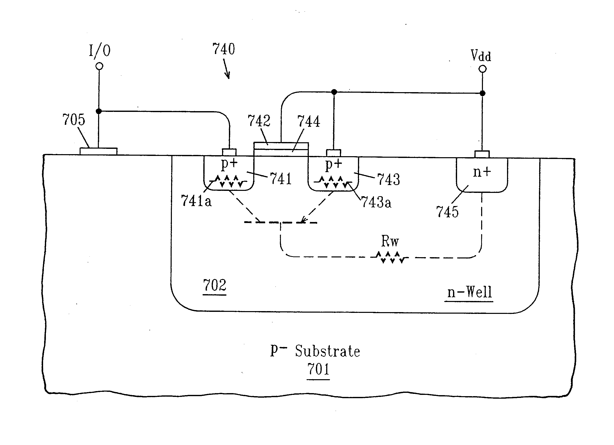
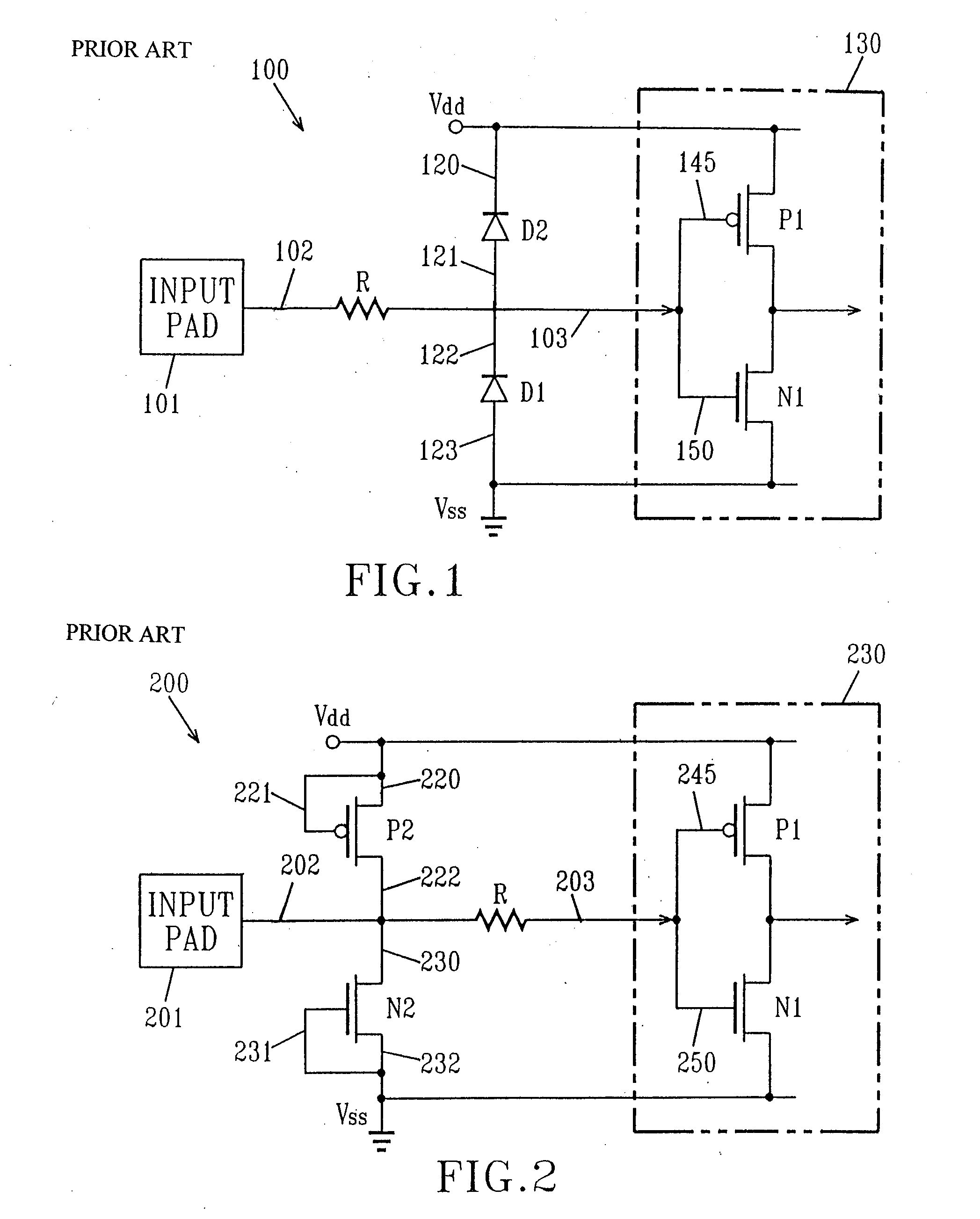
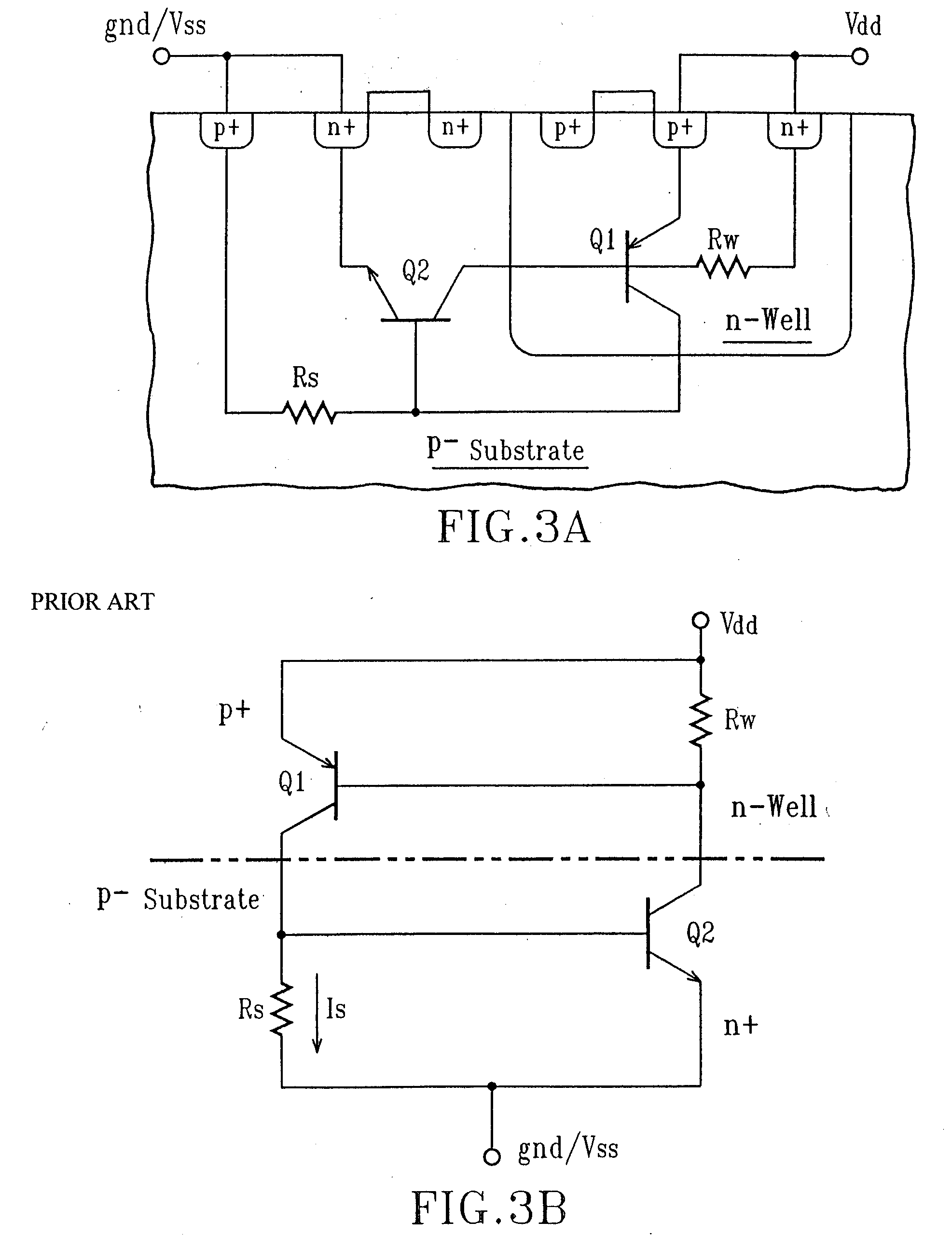
[0025] New circuit configurations described here use area efficient p-type field effect transistors to conduct current generated during an ESD event. Each disclosed p-type field effect transistor is formed within an n-well contained within a p-substrate and is silicide blocked. Silicide blocking is used to increase the level of parasitic resistance in order to improve current spread across the width of the device. Transistor connection to the I / O pad is direct so that no n-diffusions are directly connected to the I / O pad. Note that the integrated circuit within which the transistor is used may have one or more I / O cells having one or more I / O pads, with one or more of the I / O pads having latch-up robust ESD protection in accordance with the present disclosure. Note that the figures and associated description below describe connection to an input stage and pre-drive circuitry. Such connections are for illustrative purposes only in order to provide a context for the invention and shou...
PUM
 Abstract
Description
Claims
Application Information