Inductive component

a technology of inductive components and switching elements, which is applied in the direction of transformers/inductances, inductances, and continuous variable inductances/transformers, which can solve the problems of reducing the standby time or the operating time of the mobile radio device, the power of the voltage controlled oscillator is considerably impaired by the switching element, and the switching element's low series resistance is usually very large, so as to achieve hardly increase the series resistance and alter the effective inductan

Inactive Publication Date: 2005-03-10
INFINEON TECH AG
View PDF4 Cites 50 Cited by
  • Summary
  • Abstract
  • Description
  • Claims
  • Application Information

AI Technical Summary

Benefits of technology

[0014] Thus, one advantage of the invention is to be seen in the fact that the inductive component requires only a single coil which can be suitably coupled into the circuit of the inductive component in variable fashion. Consequently, the inductive component intrinsically has multiband capability without additional coils having to be connected or disconnected. This has the advantage, moreover, that hardly any additional connecting lines have to be provided in the circuit of the inductive component, as a result of which the series resistance is hardly increased.
[0015] In a preferred embodiment of the inductive component, the coil is arranged essentially in one plane. This has the advantage that the coil can be produced using planar technique. Preferably, the inductive component is integrated into an integrated circuit. Consequently, the inductive component and thus also the coil can be produced on a substrate by means of customary fabrication methods of semiconductor technique.
[0016] The coil of the inductive component preferably has a plurality of turns and also two end contacts. Preferably, the coil also has an intermediate contact that is electrically coupled to a connection. The coil then clearly represents a differential coil. The connection may be utilized for voltage supply or for current supply purposes, be grounded or remain unutilized. The two end contacts of the coil are usually electrically coupled to an AC voltage connection. Furthermore, the differential coil is preferably a fully differential coil in which the intermediate contact is provided at the center of the coil and thus represents a center contact.
[0017] The turns of the differential coil or the fully differential coil are arranged such that they are essentially transposed with one another, thereby forming partial turns. In this case, the turns are arranged essentially in the same plane, which is referred to as turns plane hereinafter. In a concrete consideration, two adjacent turns in each case cross one another at the transposition point as follows: one of the two turns changes within the turns plane from a circulation running at a first distance from the center of the coil to a circulation running at a second distance from the center of the coil. The other of the two turns changes shortly before the transposition point from the turns plane to a transposition plane running parallel, changes there below or above the transposition point from the circulation running at the second distance from the center of the coil to the circulation running at the second distance from the center of the coil and changes shortly after the transposition point from the transposition plane back to the turns plane.
[0018] In a preferred development of the inductive component, the two inner partial turns of the fully differential coil are electrically coupled to the two end contacts of the coil. In a concrete consideration, the so-called “hot ends” of the fully differential coil are thus arranged in the coil interior, that is to say at the shortest distance from the center of the fully differential coil.
[0019] Preferably, the control circuit of the inductive component has a switch element by means of which it is possible to alter the number of turns between the two tapping contacts of the coil. As a result, it is possible to alter the effective inductance between the two tapping contacts in a stepwise manner. The coil can preferably be shortened by means of the switch element in such a way that at least one outer turn of the coil can be disconnected. If a plurality of switch elements are provided in the control circuit, which switch elements are electrically coupled to the inductive component via more than two tapping contacts it is possible to alter the effective inductance in a multiplicity of steps. Consequently, an inductive component having dual band capability is produced by means of a single switch element, while a plurality of switch elements result in an inductive component having multiband capability.

Problems solved by technology

This would have the disadvantage of considerably reducing the standby time or the operating time of the mobile radio device.
In a conventional voltage controlled oscillator with a switched inductance, a disadvantage that arises is that the power of the voltage controlled oscillator is considerably impaired by the switching element.
Switching elements having a low series resistance are usually very large and load the voltage controlled oscillator with fixed additional capacitances that are not inconsiderable.
Small switching elements, by contrast, admittedly have only a low additional capacitance, but the small switching elements cause a considerable undesirable series resistance.
In the case of a voltage controlled oscillator with a switched capacitance that can be used as an alternative, a disadvantage that arises, by contrast, is that the ratio L / C is reduced instead of increased for the voltage controlled oscillator.
Consequently, the current consumption and the phase noise of the voltage controlled oscillator increase which is undesirable.
A further disadvantage is that the switched capacitance gives rise to a considerable additional series resistance with the effect mentioned above.
This plurality of coils and their connecting lines have the disadvantage that they cause a considerable space to be taken up on the substrate and, consequently, further minimization of area and reduction of costs for the mobile radio device are obstructed.

Method used


Image

  • Inductive component
  • Inductive component
  • Inductive component

Examples


Embodiment Construction

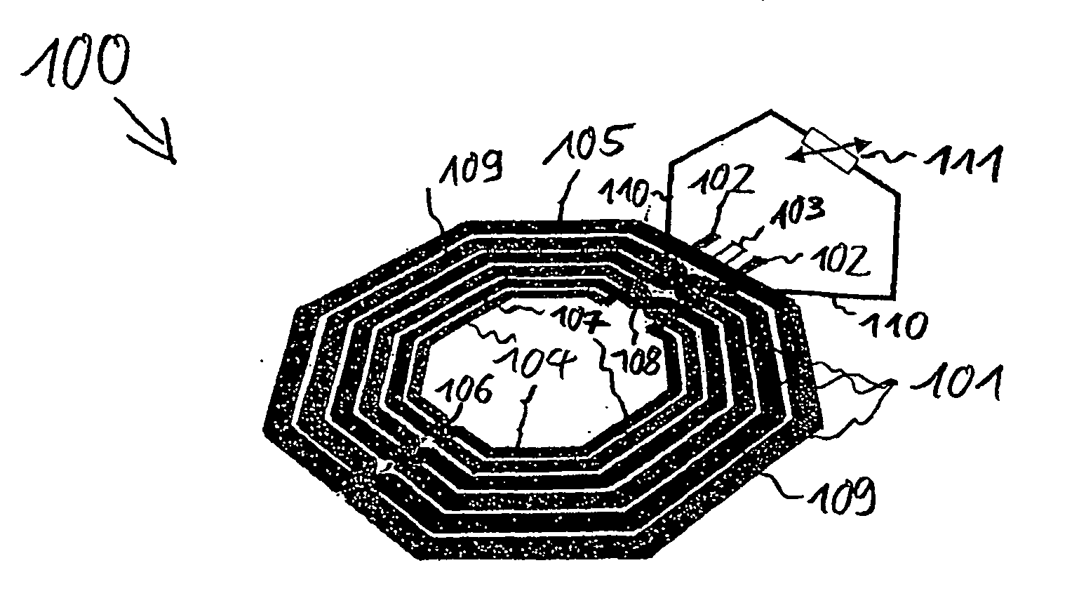
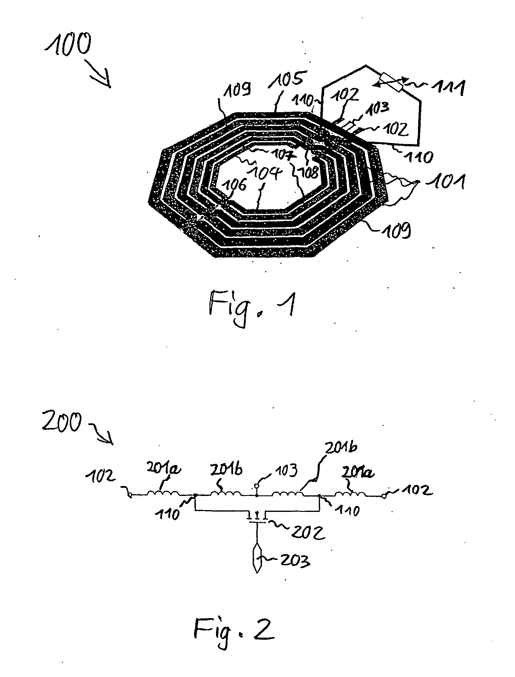
[0033]FIG. 1 shows a diagrammatic plan view of a fully differential coil 100 in accordance with a first exemplary embodiment of the invention.

[0034] The fully differential coil 100 in accordance with the first exemplary embodiment of the invention has a spiral arrangement of turns 101 which lie essentially in one plane. In accordance with the first exemplary embodiment, the turns 101 are metallic conductor tracks arranged in a metallization plane on a semiconductor substrate, in order to be able to integrate the fully differential coil 100 into an integrated circuit. Consequently, the metallization plane used for the turns 101 represents the turns plane. Furthermore, the fully differential coil 100 has two end connections 102 and a center connection 103. The total inductance of the fully differential coil 100 can be tapped off between the two end connections 102 while half the total inductance of the fully differential coil 100 can be tapped between one end connection 102 and the c...


PUM

PropertyMeasurementUnit
frequencyaaaaaaaaaa
oscillation frequencyaaaaaaaaaa

Abstract

Inductive component including precisely one coil having a total inductance and a plurality of spiral turns which are realized in the form of conductor tracks having a conductor track width that tapers toward the center of the plurality of spiral turns, two tapping contacts at the coil, and a control circuit which is connected between the two tapping contacts and alters effective inductance of the coil.

Description

CROSS-REFERENCE TO RELATED APPLICATION [0001] This application is a continuation of International Patent Application Serial No. PCT / DE02 / 04463, filed Dec. 5, 2002, which published in German on Jun. 26, 2003 as WO 03 / 052780, and is incorporated herein by reference in its entirety.FIELD OF THE INVENTION [0002] The invention relates to an inductive component. BACKGROUND OF THE INVENTION [0003] Modern mobile radio devices, for example mobile telephones, which are generally battery-operated, usually use electronic circuits. These electronic circuits use voltage controlled oscillators and should have a minimum current consumption besides minimum noise owing to the battery operation. In accordance with the prior art, for example in Cranickx J., Steyaert M. S. J.: “A 1.8-GHz Low-Phase-Noise CMOS VCO Using Optimized Hollow Spiral Inductors” in IEEE J. of Solid-State Circuits, Vol. 32, No. 5, pp. 736-744 (1997), Zannoth M., Kolb B., Fenk J., Weigel R.: “A Fully Integrated VCO at 2 GHz” in IEE...

Claims


Application Information

Patent Timeline
Patent Type & Authority Applications(United States)
IPC IPC(8): H01F17/00H01F21/12H01F27/40H01L23/522H01L23/66H01L27/08
CPCH01F17/0006H01F21/12H01F27/40H01F2017/0046H01F2021/125H01L23/5227H01L2924/0002H01L23/66H01L27/08H01L2924/00
Inventor TIEBOUT, MARC
Owner INFINEON TECH AG
Why Eureka
Try Eureka