Silicon wafers and method of fabricating the same

a technology of silicon wafers and crystalline materials, applied in the direction of crystal growth process, polycrystalline material growth, chemistry apparatus and processes, etc., can solve the problem of bulk micro-defects (bmd) and other problems

Active Publication Date: 2005-03-10
SK HYNIX INC +1
View PDF11 Cites 37 Cited by
  • Summary
  • Abstract
  • Description
  • Claims
  • Application Information

AI Technical Summary

Benefits of technology

[0020] In another refinement, a disclosed method of fabricating a silicon wafer comprised: preparing a silicon wafer having a front surface, a back surface, a circumferential edge portion, and a bulk region between the front and back surfaces; performing a first rapid thermal process to consume vacancies in the silicon wafer, thereby ac

Problems solved by technology

In refinement, the defects may be bulk micro-defects (BMD

Method used


Image

  • Silicon wafers and method of fabricating the same
  • Silicon wafers and method of fabricating the same
  • Silicon wafers and method of fabricating the same

Examples


Embodiment Construction

[0057] Certain preferred embodiments will be described with reference to the accompanying drawings. Since these embodiments are provided only for the purpose of providing those of ordinary skilled in the art with an understanding of this disclosure, it will be noted that they may be modified in various manners and that the scope of this disclosure is not limited by the embodiment described herein.

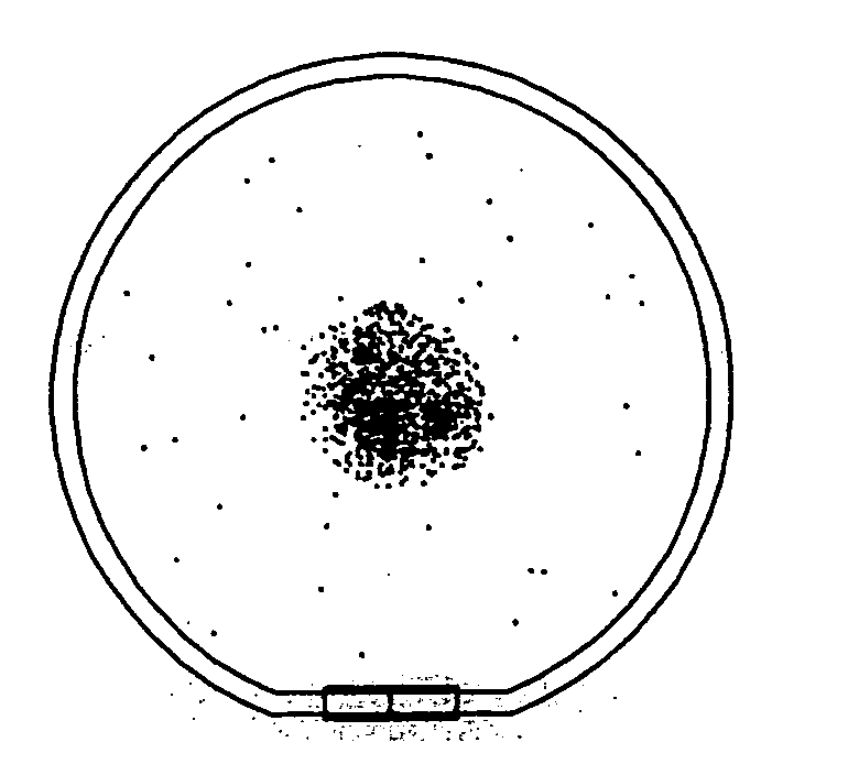
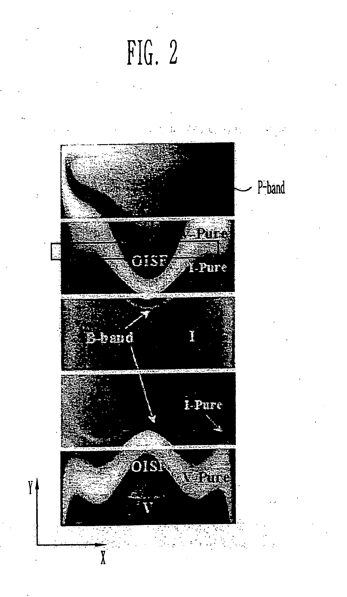
[0058] By using a two-step RTP (rapid thermal processing) process, a wafer with an ideal semiconductor device region is provided by controlling fine oxygen precipitates and OiSFs (Oxidation Induced Stacking Fault) located on the surface region of the wafer. By performing the two-step rapid thermal process, the distribution of defects can be accurately controlled and an ideal device active zone can be formed up to a certain depth from the surface of the wafer. In addition, it is possible to maximize the internal gettering (IG) efficiency by enabling the oxygen precipitates and the bulk stac...


PUM


Abstract

By using a two-step RTP (rapid thermal processing) process, the wafer is provided which has an ideal semiconductor device region secured by controlling fine oxygen precipitates and OiSFs (Oxidation Induced Stacking Fault) located on the surface region of the wafer. By performing the disclosed two-step rapid thermal process, the distribution of defects can be accurately controlled and an ideal device active zone can be formed up to a certain distance from the surfaces of the wafer. In addition, it is possible to maximize the internal gettering (IG) efficiency by enabling the oxygen precipitates and the bulk stacking faults to have constant densities in the depth direction in an internal region of the wafer, that is, the bulk region. In order to obtain the constant concentration profile of the oxygen precipitates and the bulk stacking faults in the bulk region, the wafer is subjected to the aforementioned two-step rapid thermal process in a predetermined mixed gas atmosphere.

Description

BACKGROUND [0001] 1. Technical Field [0002] Improved silicon wafers and methods of fabricating silicon wafers are disclosed. More specifically, silicon wafers with an ideal device active zones formed up to a certain distance from the front and rear surfaces of the wafer and with an internal region that has a constant density of oxygen precipitates and bulk stacking faults in a depth direction and a method of fabricating the silicon wafer are disclosed. [0003] 2. Description of the Related Art [0004] Generally known defects causing problems in a silicon wafer include COPs (Crystal Originated Particle), FPDs (Flow Pattern Defect), and LSTDs (Laser Scattering Tomography Defect). [0005] The COPs formed in a surface layer of the wafer are detected by repeating a cleaning process with a mixed solution (Standard Cleaning 1 solution) of ammonia and hydrogen peroxide. The COPs have sizes in a range of about 0.09 μm to about 0.12 μm and are observed in shapes of pits on the surface of the waf...

Claims


Application Information

Patent Timeline
IPC IPC(8): H01L21/00C30B29/06H01L21/02H01L21/322H01L21/324
CPCH01L21/324H01L21/3225C30B29/06
Inventor MUN, YOUNG HEEKIM, KUNKOH, CHUNG GEUNPYI, SEUNG HO
Owner SK HYNIX INC
Why Eureka
Try Eureka