Defect-tolerant and fault-tolerant circuit interconnections

a fault-tolerant and interconnection technology, applied in the field of nanoscale electronic circuits, can solve the problems of many alignment and spontaneous defect problems, the yield of usable combination nanoscale/microscale circuits is too low to be economically viable, and the interface between essentially non-defective microelectronic circuitry and nanoelectronic circuitry is problematic. to achieve the effect of increasing the voltage or current separation

Active Publication Date: 2005-03-10
VALTRUS INNOVATIONS LTD +1
View PDF6 Cites 67 Cited by
  • Summary
  • Abstract
  • Description
  • Claims
  • Application Information

AI Technical Summary

Benefits of technology

One embodiment of the present invention is an electronic memory comprising an array of nanowire crossbars, the nanoscale memory elements within the nanowire crossbars addressed through conventional microelectronic address lines. In order to interconnect the microelectronic address lines with the nanowire crossbars, an address encoding technique is employed to generate a number of redundant address lines to supplement a minimally required set of address signal lines needed to access the nanoscale memory elements. The supplemental address lines allow for unique memory-element addressing in the presence of significant nanowire-to-microelectronic-address-line interconnect...

Problems solved by technology

However, many alignment and spontaneous defect problems need to be overcome to successfully manufacture electronic devices that include nanoelectronic circuits, including nanowire crossbars.
The interface between essentially non-defective microelectronic circuitry and nanoelectronic circuitry is problematic.
The relatively high manufacturing-defect rate that occurs in fabricating nanoelectronic devices may produce a yield of usable combination nanoscale/microscale circuits too low to be economically viable.
However, it is not feasible to extend existing redundancy-based, defect avoidance strategies designed for nanoscale circuits to microelectronic circuitry through nanoscale-to-microscale interfaces, because these redundancy-based techniques depend on an ability to attempt a measurement of each junction in the nanoscale circuits to determine whether or not the junction is defective.
Thus, defects in the interconnection interface result in degradation or complete lack of addressability of interconnection interface components.
The interconnection interface may be viewed as a type of bootstrap mechanism that allows defect control in a nanoscale circuit, the components of which are addressed through the bootstrap For example, electronic memories based on nanowire-crossbar-implemented memory-element arrays are attractive with respect to size and power co...

Method used


Image

  • Defect-tolerant and fault-tolerant circuit interconnections
  • Defect-tolerant and fault-tolerant circuit interconnections
  • Defect-tolerant and fault-tolerant circuit interconnections

Examples


Embodiment Construction

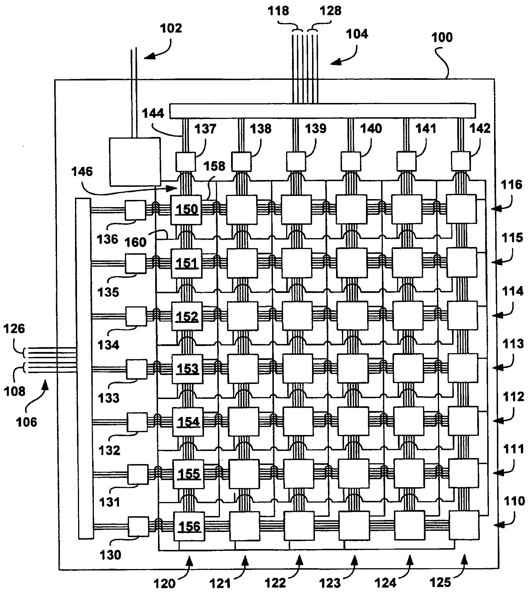
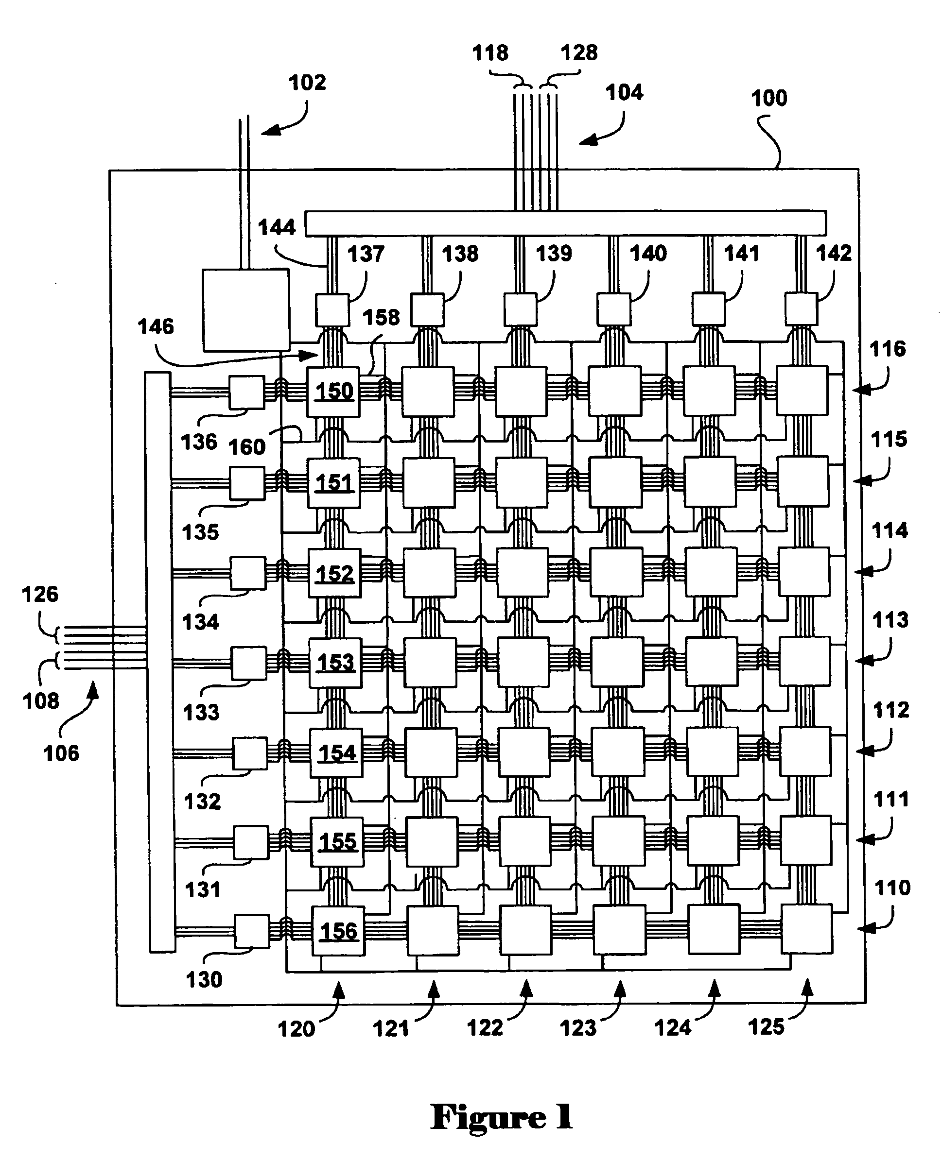
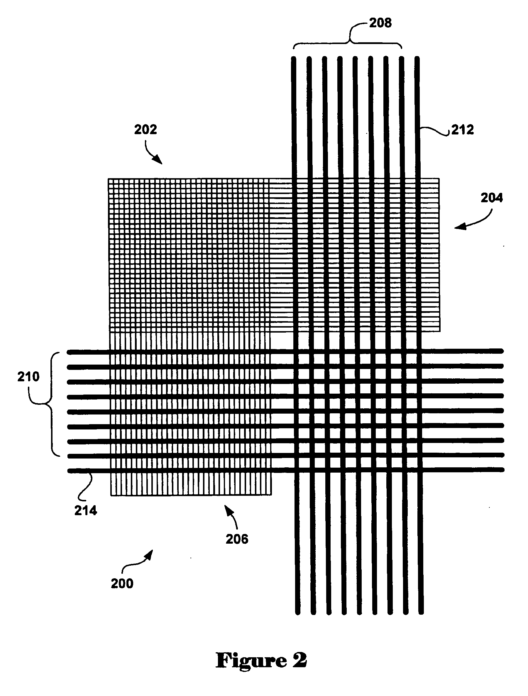
Various embodiments of the present invention include a combined nanoscale / microscale electronic memory device and fault-tolerant interconnections between microelectronic circuits and nanoelectronic circuits within the electronic memory. Techniques for determining, in one described approach, nanoelectronic-to-microelectronic interface topologies employ concepts and mathematical techniques developed for error-control coding used in various data-transmission applications. Therefore, in a first subsection, a mathematical description of a number of error-control encoding techniques is provided. In a second subsection, a partially nanoscale electronic memory that represents one embodiment of the present invention is described. In a third subsection, a method for determining the nanoelectronic-to-microelectronic circuit-interface topologies within the electronic memory are described.

Mathematical Description of Selected Error-Control Encoding Techniques

Embodiments of the present inventi...


PUM


Abstract

Methods for increasing defect tolerance and fault tolerance in systems containing interconnected components, in which a signal level is classified as belonging to one of a plurality of different, distinguishable classes based on one or more thresholds separating the signal-level classes, and defect-and-fault tolerant systems embodying the methods. An electronic-device embodiment including an array of nanowire crossbars, the nanoscale memory elements within the nanowire crossbars addressed through conventional microelectronic address lines, and a method embodiment for providing fault-tolerant interconnection interfaces with electrically distinguishable signal levels are described. In the described embodiment, in order to interconnect microelectronic address lines with the nanowire crossbars within the electronic memory, an address encoding technique is employed to generate a number of redundant, parity-check address lines to supplement a minimally required set of address signal lines needed to access the nanoscale memory elements.

Description

TECHNICAL FIELD The present invention relates to nanoscale electronic circuits and, in particular, to defect-tolerant interconnection interfaces with electrically distinguishable signal levels, including interfaces between microelectronic and nanoelectronic circuits used in a combination nanoscale / microscale electronic memory, combination nanoscale / microscale logic circuits, field-programmable gate arrays, and processors. BACKGROUND OF THE INVENTION The present invention is related to nanoscale electronic circuit interconnections, including memory devices employing nanowire crossbars and defect-tolerant interconnections with electrically distinguishable signal levels between microelectronic circuit elements and nanowires. Nanowire crossbar technologies, and a variety of nanoscale electronic circuits, are discussed in a number of issued U.S. patents and filed U.S. patent applications, including (1) U.S. Pat. No. 6,459,095, entitled “Chemically Synthesized and Assembled Electronic D...

Claims


Application Information

Patent Timeline
IPC IPC(8): G06F11/10G11C8/10G11C8/20G11C13/00
CPCB82Y10/00G06F11/1016G11C2213/81G11C13/0014G11C2213/77G11C8/10
Inventor KUEKES, PHILIP J.SEROUSSI, GADIELWILLIAMS, RICHARD STANLEY
Owner VALTRUS INNOVATIONS LTD
Why Eureka
Try Eureka