Optical device, and process for producing it

a technology of optical devices and optical waveguides, applied in the direction of optical waveguide light guides, optical elements, instruments, etc., can solve the problems of high losses of waveguides, lack of sharp or readily definable refractive index profiles, and diffusion of ions in substrates, etc., to achieve the effect of improving attenuation properties

Inactive Publication Date: 2005-03-17
SCHOTT AG
View PDF4 Cites 53 Cited by
  • Summary
  • Abstract
  • Description
  • Claims
  • Application Information

AI Technical Summary

Benefits of technology

[0024] An optical device of this type, which as light-guiding structure has a section of the substrate which is raised with respect to adjacent regions, has the benefit compared to known devices produced by ion exchange that the structure has interfaces with the surrounding medium which are perpendicular or at least inclined with respect to the adjacent substrate surface. Accordingly, a high difference in refractive index is achieved in a direction along the substrate surface, with the result that structures of this type produced in accordance with the invention have a greatly reduced attenuation at bends or corners running along the surface.
[0029] According to a preferred embodiment of the invention, the step of exchanging substrate ions also comprises the step of heating the substrate, in order to increase the mobility of the ions and thereby to accelerate the exchange process.
[0030] Moreover, in a simple way the coating of the at least one first region of the substrate with a coating comprising the first layer can be effected by photolithographic patterning of the coating. It may also be advantageous for the step of removing substrate material from at least one region that adjoins the first region to comprise the step of photolithographic patterning of the substrate.
[0037] Furthermore, according to a particularly preferred embodiment of the process according to the invention, the step of exchanging substrate ions with exchange ions from the first layer comprises the step of field-assisted exchange of substrate ions with exchange ions from the first layer. The field assistance results in even better definition of the refractive index profile and / or of the interfaces of an optical element produced in accordance with the invention. In particular, in the region of the elevated first region the electric field runs substantially perpendicular to the surface, whereas at the height of the surface of the recessed second region, or at the base of the raised structure of the first region, the electric field fans out extensively. This also leads to extensive dilution of the exchange ions at this location, with the result that the drop in concentration of exchange ions which occurs as a result produces a relatively sharp change in the refractive index.
[0042] By way of example, it is advantageous if at least a second layer is also present during field-assisted ion exchange. This ensures that the voltage supply is maintained even when the layer is diluted by the exchange atoms as a result of the exchange process, ultimately losing its conductivity.
[0046] The at least one second region, which has been recessed with respect to the first region by removal of substrate material, can also then be filled again. It is also possible, for example in order to protect the structures produced on the substrate and to optimize the optical mode field, for the substrate to be covered, in particular on a side having an optical element which has been produced in accordance with the invention, by coating with a transparent material after the ion exchange.

Problems solved by technology

The diffusion of the ions in the substrate, however, does not provide a sharp or readily definable refractive index profile.
In particular, high losses are encountered if the waveguides do not run purely in a straight line, but rather also include curves.
However, such curves can scarcely be avoided in integrated optical devices, such as for example a Mach Zehnder interferometer.
The losses are also caused by the fact that ion exchange can only be used to build up relatively slight differences in refractive index, and consequently light-guiding structures produced by ion exchange have only a small numerical aperture.

Method used


Image

  • Optical device, and process for producing it
  • Optical device, and process for producing it
  • Optical device, and process for producing it

Examples


Embodiment Construction

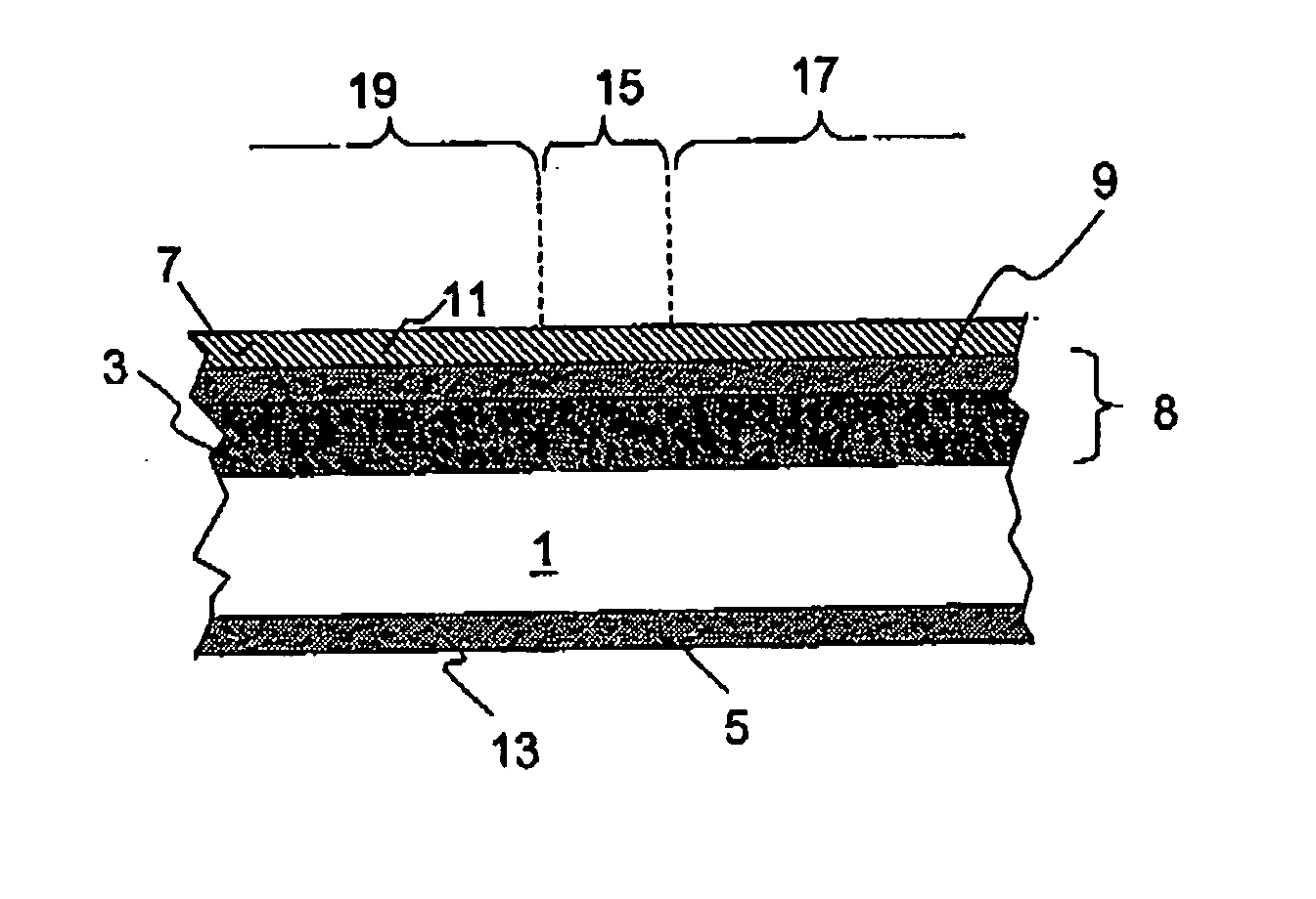
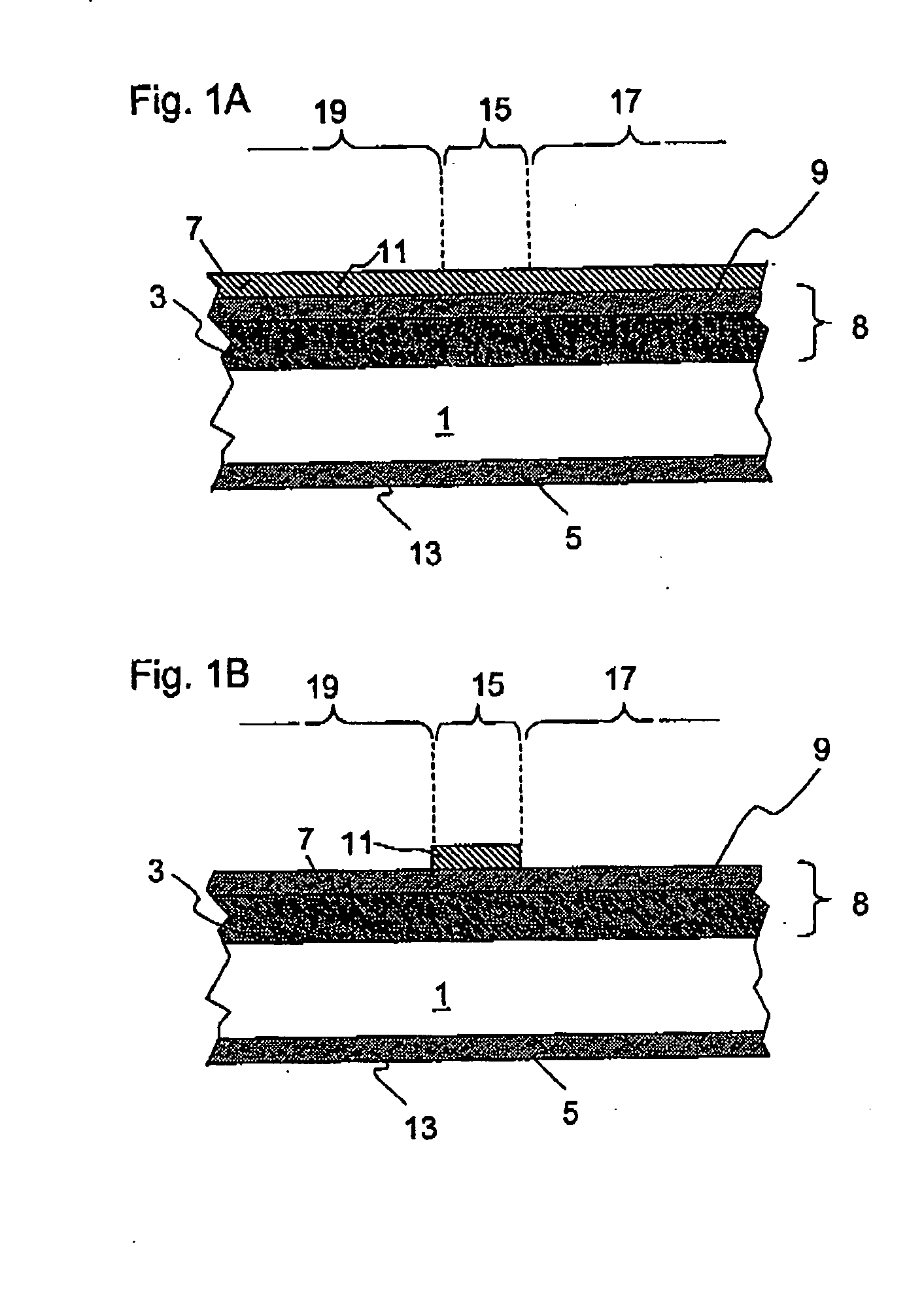
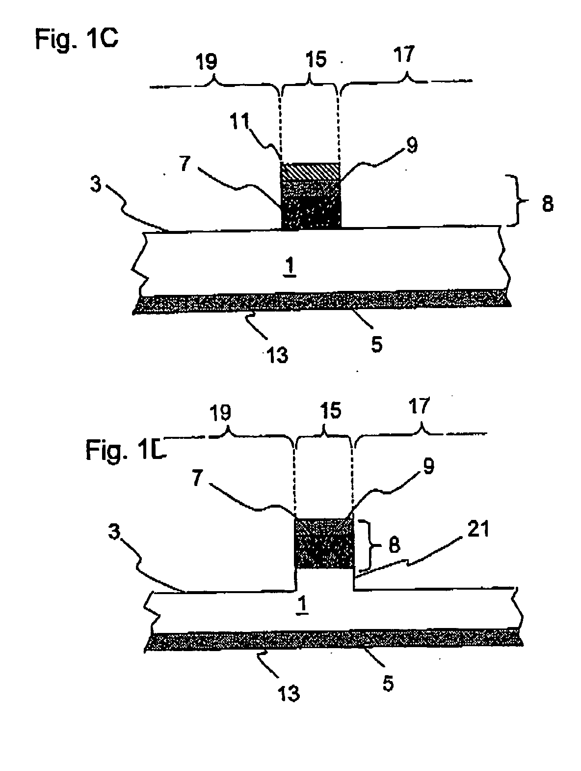
[0063]FIG. 1A to 1F use schematic cross-sectional views to show the steps involved in one embodiment of the process according to the invention for producing an optical device according to the invention.

[0064] First of all, a substrate 1 is provided with a coating 8 on a first side 3. This coating comprises a first layer 7, which includes exchange atoms in neutral or ionic form. The layer 7 may in this case, by way of example, be a metallic silver layer. It is preferable for the first layer to be applied with a thickness in a range from 20 nm to 1200 nm, preferably in a range from 100 to 600 nm.

[0065] The coating 8 also comprises a second layer 9, which is applied to the first layer 7, so that the first layer 7 is in contact with the surface of the substrate 1. The second layer 9 applied may, for example, be a titanium layer, a chromium layer, an aluminum layer or a copper layer. According to a preferred embodiment of the process, the coating 8 comprising the individual layers 7 an...


PUM

PropertyMeasurementUnit
thicknessaaaaaaaaaa
thicknessaaaaaaaaaa
thicknessaaaaaaaaaa

Abstract

A process for producing an optical device by means of ion exchange is provided. The method includes: coating at least one first region of a substrate with a coating having a first layer of exchange atoms in neutral or ionic form; removing substrate material from at least one second region that adjoins the first region; and exchanging substrate ions with exchange ions from the first layer.

Description

BACKGROUND OF THE INVENTION [0001] 1. Field of the Invention [0002] The invention relates in general terms to optical devices and to the production thereof, in particular the production of optical elements by means of ion exchange. [0003] 2. Description of Related Art [0004] Since electrical signal transmission with increasing data transmission rates is reaching its limits, optical signal transmission methods are becoming increasingly important, in particular in the field of data transfer. As part of this development, in addition to signal transfer there has also been an increasing demand for devices for optical signal processing. To satisfy this demand, the concept of integrated optics was proposed by S. E. Miller as early as 1969. Waveguides generally form the base elements for devices of this type. [0005] To produce integrated optical devices, it is in many cases necessary to combine a plurality of waveguides within a tight space. For this purpose, the waveguides and other elemen...

Claims


Application Information

Patent Timeline
Patent Type & Authority Applications(United States)
IPC IPC(8): C03C15/00C03C17/34C03C21/00G02B6/12G02B6/134G02B6/34
CPCC03C15/00C03C17/34C03C21/002C03C21/003C03C2217/91G02B2006/12176G02B6/1345G02B2006/12097G02B2006/1215G02B2006/12159G02B6/12014
Inventor BRINKMANN, MATTHIASPAWLOWSKI, EDGARTHOMA, FRANKWOYWOD, TANJABEIER, WOLFRAM
Owner SCHOTT AG
Why Eureka
Try Eureka