Dual depth trench termination method for improving Cu-based interconnect integrity

Active Publication Date: 2005-03-17
TEXAS INSTR INC
View PDF8 Cites 0 Cited by
  • Summary
  • Abstract
  • Description
  • Claims
  • Application Information

AI Technical Summary

Benefits of technology

[0004] A dielectric layer is formed over a semiconductor. Any number of intervening layers can be formed between the semiconductor and the dielectric layer. A plurality of vias, separated by a minimum distance XV, is formed in the dielectric layer to allow the subsequently formed copper layer to contact an underlying copper layer. A trench is formed in the dielectric layer over the plurality of vias with an edge that extends a minimum distance of XTO from the edge α of the via closest to the edge of the trench. The trench can comprise a depth d1 in the region containing the vias and a depth d2 at the edge of the trench. In general the condition d1>d2 will apply to the depths of the trench. The trench and vias will be filled with copper to form a copper interconnect line. The minimum overhang of the copper line will reduce and / or eliminate the copper delamination the currently occurs.

Problems solved by technology

Copper delamination is a major problem that affects the reliability and operation of the integrated circuit.
This delamination can cause the integrated circuit to become inoperable and fail.

Method used


Image

  • Dual depth trench termination method for improving Cu-based interconnect integrity
  • Dual depth trench termination method for improving Cu-based interconnect integrity
  • Dual depth trench termination method for improving Cu-based interconnect integrity

Examples


Embodiment Construction

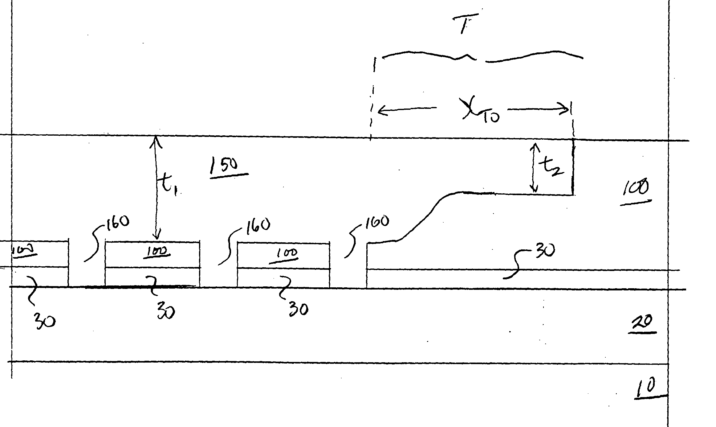
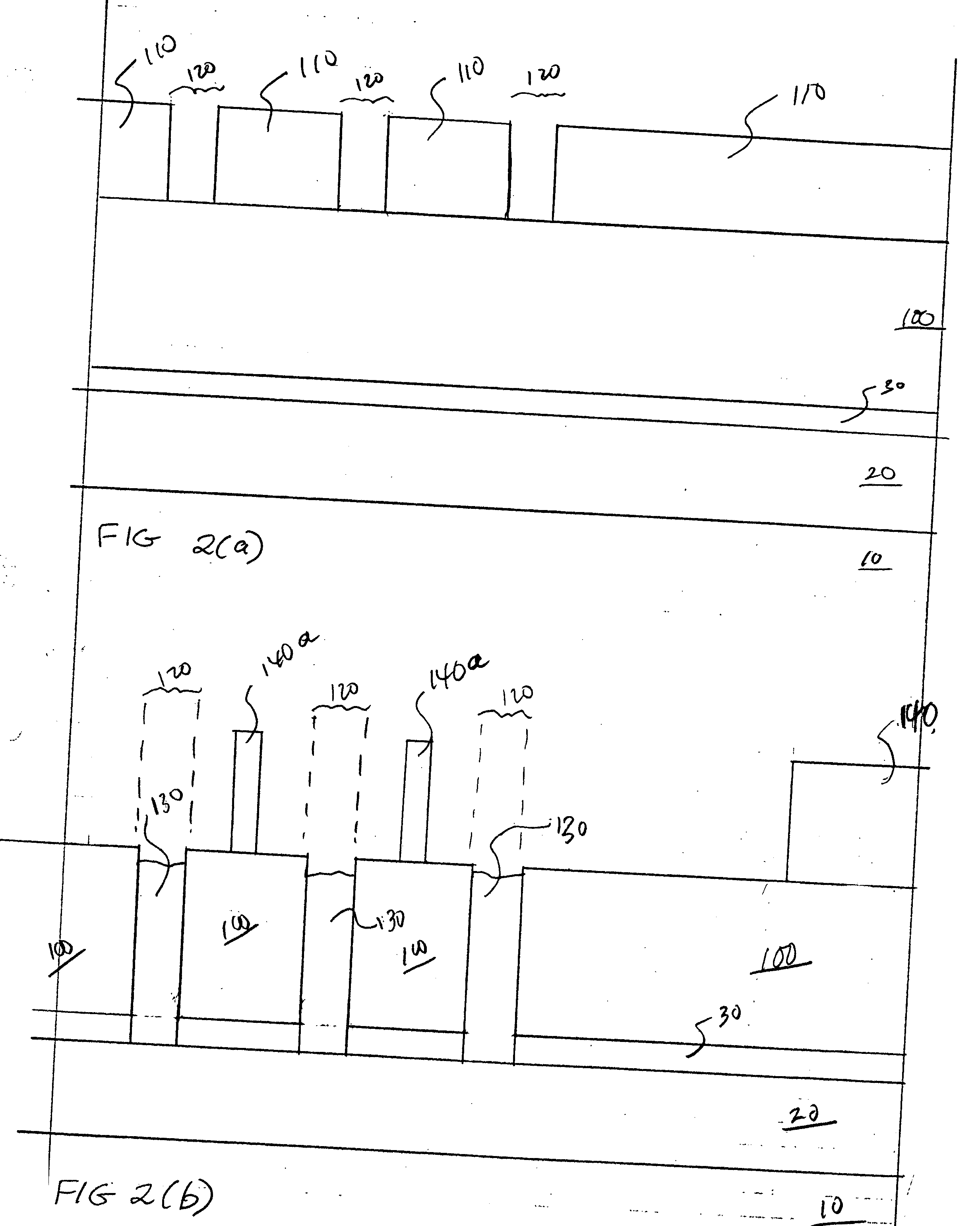
[0010] While the following description of the instant invention revolves around FIG. 2(a) to FIG. 2(f), the instant invention can be utilized in many semiconductor device structures. The methodology of the instant invention provides a solution to forming reliable copper interconnect structures.

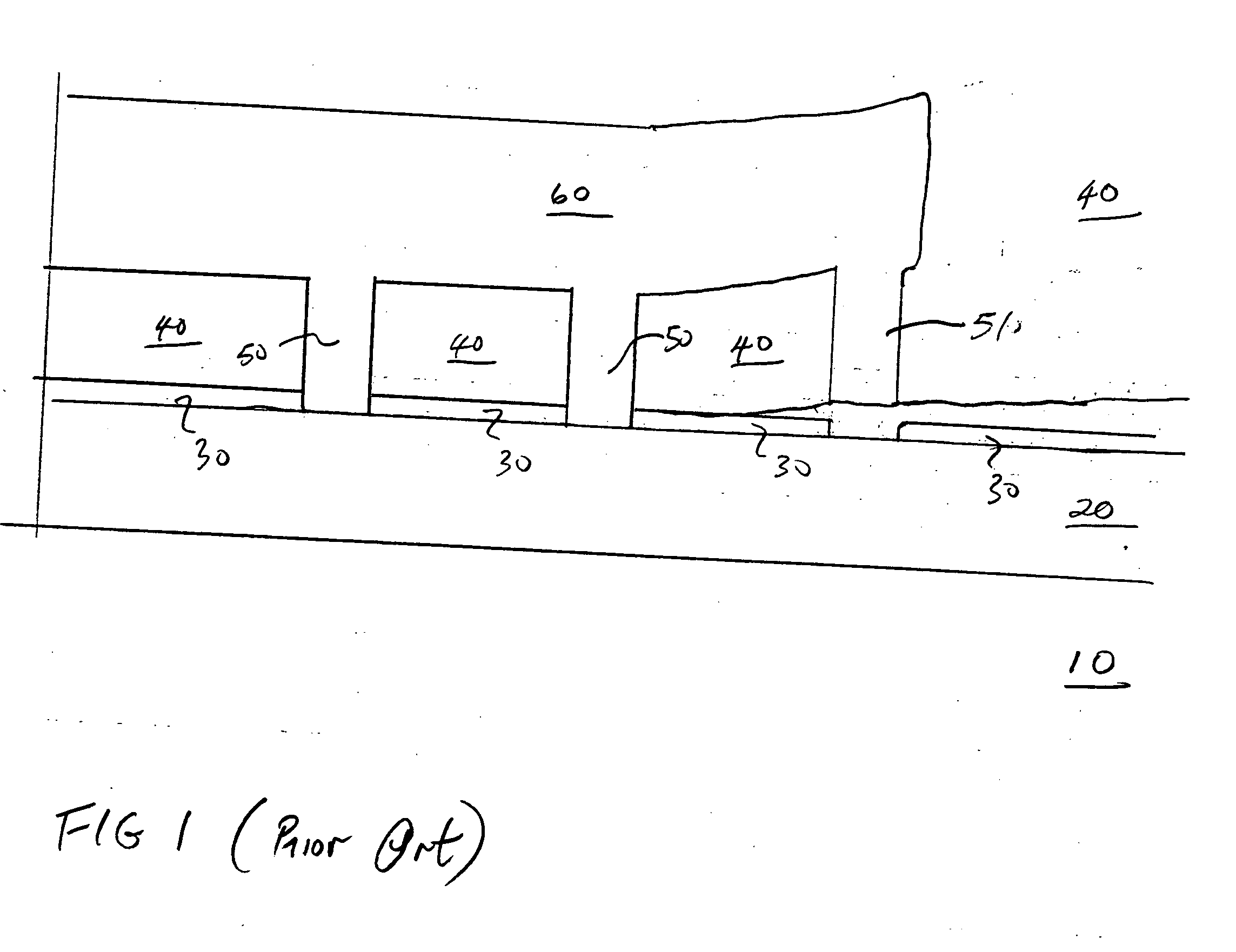
[0011] An embodiment of the instant invention will now be described by referring to FIG. 2(a) to FIG. 2(d). As shown in FIG. 2(a), a copper metal layer 20 is formed on a dielectric layer 10. The dielectric layer 10 is formed over a semiconductor. Electronic devices such as transistors, capacitors, and diodes will be formed in the semiconductor. In addition there may be any number of intervening layers and structures between the semiconductor and the dielectric layer 10. The semiconductor and any intervening layers have been omitted for clarity. Following the formation of the copper layer 20, a barrier layer 30 is formed on the copper layer 20. This barrier layer can comprise silicon nitride o...


PUM


Abstract

A trench is formed in a low K dielectric (100) over a plurality of vias (120) also formed in the low K dielectric layer (100). The vias are separated by a distance of less than XV and the edge of the trench is greater than XTO from the edge α of the via closest to the edge of the trench. The trench and vias are subsequently filled with copper (150), (160) to form the interconnect line.

Description

FIELD OF THE INVENTION [0001] The invention is generally related to the field of integrated circuits and more specifically to a dual trench depth termination method for improving the integrity of Cu-based semiconductor interconnects. BACKGROUND OF THE INVENTION [0002] High performance integrated circuits utilize low K dielectric layers and copper metal to form the lines that interconnect the various electronic devices that comprise the circuit. The copper interconnect lines comprise copper formed in trenches and vias in the low K dielectric material. [0003] Illustrated in FIG. 1 is a cross section diagram of a typical copper interconnect structure showing copper delamination. Copper delamination is a major problem that affects the reliability and operation of the integrated circuit. As shown in FIG. 1, a dielectric layer 10 is formed over a semiconductor. Electronic devices such as transistors, capacitors, and diodes will be formed in the semiconductor. In addition there may be any ...

Claims


Application Information

Patent Timeline
IPC IPC(8): H01L21/768
CPCH01L21/76808
Inventor TIWARI, RAJESHFIELDS, RUSSELLBODDICKER, SCOTT A.KIM, ANDREW TAE
Owner TEXAS INSTR INC
Why Eureka
Try Eureka