High brightness light emitting diode

a light-emitting diode and high-brightness technology, which is applied in the direction of electrical apparatus, semiconductor/solid-state device manufacturing, and semiconductor devices, etc., can solve the problems of reducing production yield, difficult lattice alignment, and not contributing to the brightness of leds, etc., to achieve excellent reflectivity, brightness and yield of leds of the present invention, and promote the effect of excellent reflectivity

Inactive Publication Date: 2005-03-24
NAT SCI COUNCIL
View PDF6 Cites 19 Cited by
  • Summary
  • Abstract
  • Description
  • Claims
  • Application Information

AI Technical Summary

Benefits of technology

[0009] The object of the present invention is to provide a high brightness light emitting diode (LED), in which gallium phosphide is provided as a window and thus promote the brightness.
[0016] According to the above method, an LED composed of a GaP window and a reflective mirror with excellent reflectivity will be completed. Furthermore, brightness and yield of the LED of the present invention are promoted.

Problems solved by technology

The GaP material is provided here, but unfortunately doesn't contribute to brightness of the LED.
However, lattice alignment is difficult and bonding directly to the epitaxial layer at high temperature will seriously decrease production yield.

Method used


Image

  • High brightness light emitting diode
  • High brightness light emitting diode
  • High brightness light emitting diode

Examples


Embodiment Construction

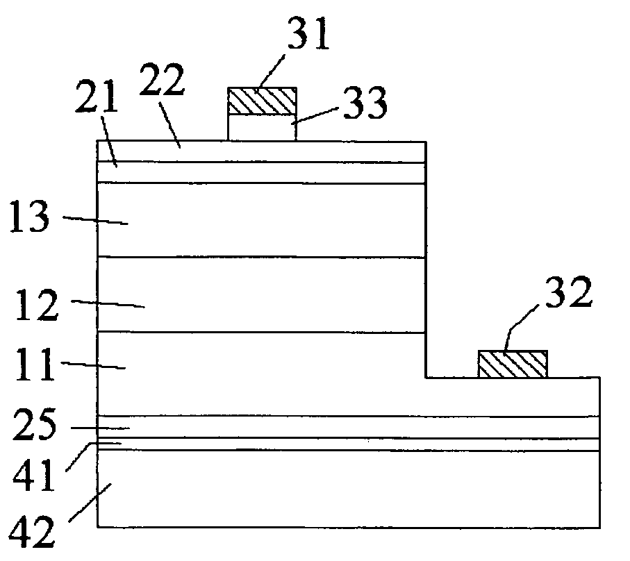
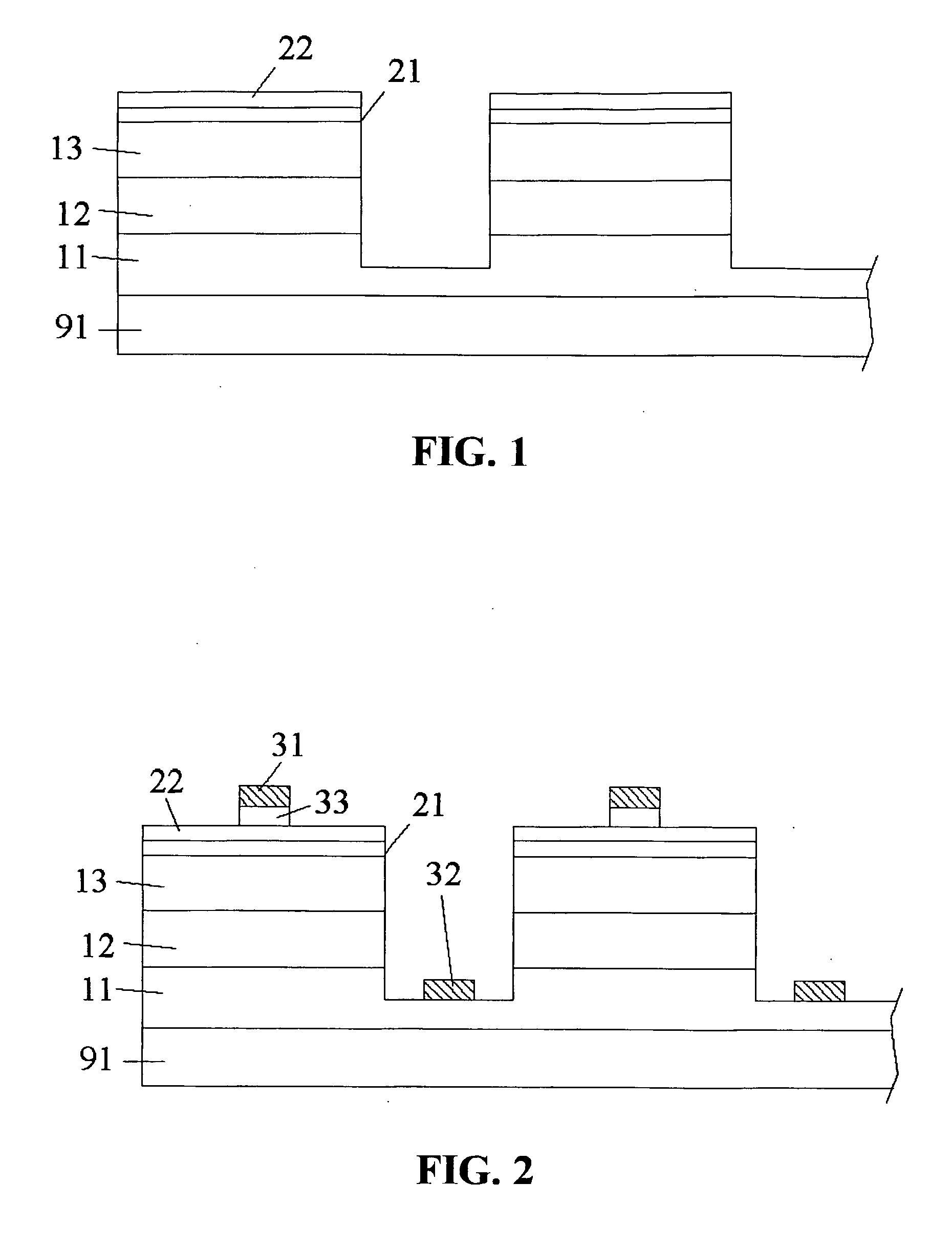
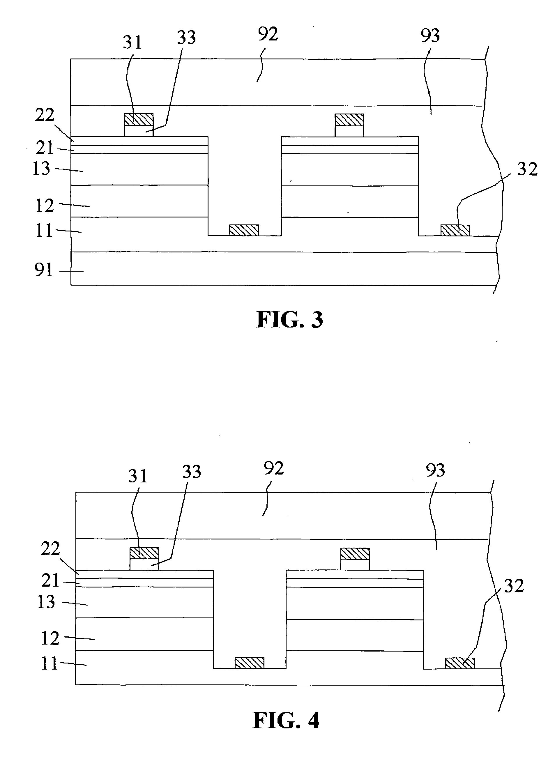
[0019]FIGS. 1-7 illustrate the processes for producing the LED of the present invention. First, on a GaAs temporary substrate 91, a multilayered structure sequentially including a first cladding layer 11 of n-AlGaInP, an active layer 12 of undoped AlGaInP, and a second cladding layer 13 of p-AlGaInP, is formed by MOVPE, as shown in FIG. 1.

[0020] In general, the active layer 12 can be formed by III-V or II-VI compounds with a pn (or np) junction and direct-bandgap. In this embodiment, undoped AlGaInP having wavelength ranging from 550 nm to 630 nm is used. AlGaInP can be expressed as (AlxGa1-x)0.5In0.5P, wherein 0.5≦x≦1 for both of the cladding layers 11, 13; and 0≦x≦0.45 for the active layer 12.

[0021] On the second cladding layer 13, the transparent p-GaP layer 21 is epitaxed to about 0.2-60 μm thick. The GaP layer 21 has a bandgap larger than the LED epitaxial layer, and therefore exhibits good transparency at wavelength of red to green light. The GaP layer 21 also facilitates cu...


PUM


Abstract

The present invention discloses a high brightness light emitting diode. The light emitting diode primarily includes a permanent substrate, a reflective mirror formed on said permanent substrate, an n-type cladding layer formed on said reflective mirror, and defining a higher port and a lower port on an upper surface thereof, an active layer with quantum well structure formed on said higher port of said n-type cladding layer, a p-type cladding layer formed on said active layer, a p-GaP layer formed on said p-type cladding layer, a metal contact layer formed on said GaP layer, a p-type ohmic contact electrode formed on said metal contact layer, and an n-type ohmic contact electrode formed on said lower port of said n-type cladding layer. By providing a gallium phosphide window and a reflective mirror, brightness of the LED can be promoted.

Description

CROSS REFERENCE [0001] The present application is a Division of co-pending U.S. application Ser. No. 10 / 668,554 by the same inventors filed on Sep. 22, 2003.BACKGROUND OF THE INVENTION [0002] 1. Field of the Invention [0003] The present invention relates to a high brightness light emitting diode, in which gallium phosphide is provided as a window. [0004] 2. Related Prior Art [0005] For manufacturing light emitting diodes, it's very important to promote brightness. Gallium phosphide (GaP) is a material with good electrical conductivity and high transparency in wavelength ranging from red to green, and therefore frequently applied to light emitting diodes (LEDs). [0006]FIG. 8 shows a conventional LED structure including GaP. In this structure, a SiO2 layer 82, a reflective metal layer 83, a GaP layer 84, an active layer 85 and a gallium arsenide (GaAs) window 86 are sequentially presented on the silicon substrate 81. The electrodes 87, 88 are respectively formed on the GaAs window 86 ...

Claims


Application Information

Patent Timeline
Patent Type & Authority Applications(United States)
IPC IPC(8): H01L33/00
CPCH01L33/0079H01L33/0093
Inventor HORNG, RAY-HUAWU, DONG-SINGCHIANG, YANN-JYHCHIU, CHI-YING
Owner NAT SCI COUNCIL
Why Eureka
Try Eureka