Field-effect transistors with weakly coupled layered inorganic semiconductors

a field-effect transistor and inorganic semiconductor technology, applied in the field of field-effect transistors, can solve the problems of undesirable properties of crystalline silicon-based fets for some electronics applications, affecting the operation of fets, and their operating characteristics are typically substantially inferior to those of crystalline silicon-based fets, and achieves mechanical flexibility and high mobilities.

Inactive Publication Date: 2005-03-24
RUTGERS THE STATE UNIV +1
View PDF5 Cites 55 Cited by
  • Summary
  • Abstract
  • Description
  • Claims
  • Application Information

AI Technical Summary

Benefits of technology

[0008] Various embodiments provide inorganic FETs in which the semiconductor channels include a material having anisotropic chemical bonding. Due to the anisotropic chemical bonding, the semiconductor channels have high mobilities and also exhibit mechanical flexibility.

Problems solved by technology

For that reason, high densities of trapped charge densities adversely affect operation of an FET.
Though the passivation step enables the fabrication of crystalline silicon-based FETs with excellent operating characteristics, crystalline silicon-based FETs have one property that is undesirable for some electronics applications.
While organic FETs are flexible and have been fabricated on flexible substrates, their operating characteristics are typically substantially inferior to those of crystalline silicon-based FETs.

Method used


Image

  • Field-effect transistors with weakly coupled layered inorganic semiconductors
  • Field-effect transistors with weakly coupled layered inorganic semiconductors
  • Field-effect transistors with weakly coupled layered inorganic semiconductors

Examples


Embodiment Construction

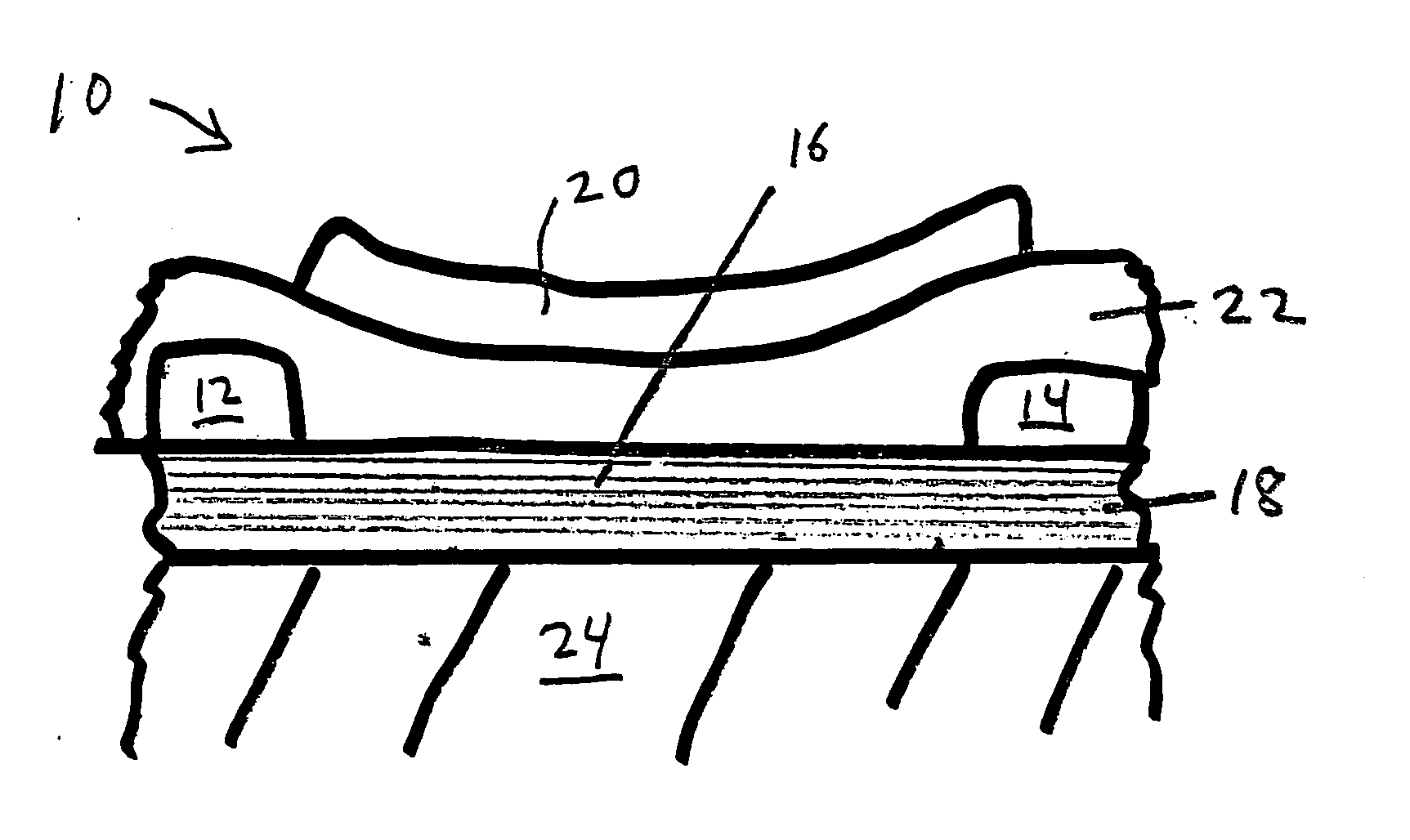
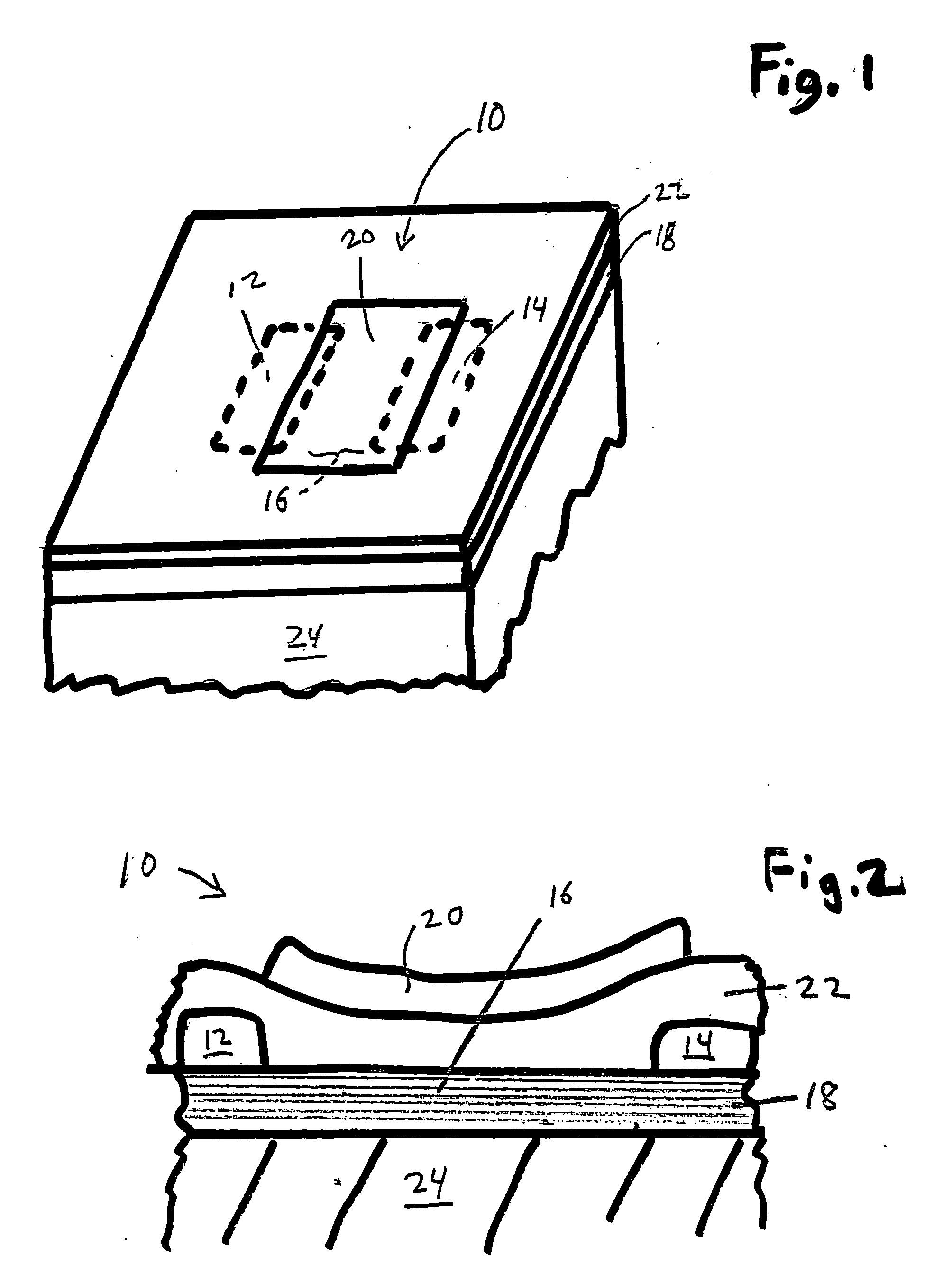
[0022]FIGS. 1-2 show a field-effect transistor (FET) 10 with an inorganic semiconductor. The FET 10 includes source and drain electrodes 12, 14. Exemplary source and drain electrodes are fabricated of metal, e.g., as silver, gold, copper, or aluminum or of a conductive material such as carbon or heavily doped semiconductor. The source and drain electrodes 12, 14 provide electrical connections to ends of an active semiconductor channel 16. The active semiconductor channel 16 is a portion of a layer 18 of highly anisotropically bonded inorganic semiconductor. The FET 10 also includes a control gate structure, which includes a gate electrode 20 and a gate dielectric layer 22. Exemplary conductors for the gate electrode 20 include conductors listed above for the source and drain electrodes 12, 14. The gate dielectric layer 22 is interposed between the gate electrode 20 and the layer 18 of highly anisotropically bonded inorganic semiconductor. Exemplary gate dielectric layers 22 are form...


PUM


Abstract

A field-effect transistor includes source, drain, and gate electrodes; a crystalline or polycrystalline layer of inorganic semiconductor; and a dielectric layer. The layer of inorganic semiconductor has an active channel portion physically extending from the source electrode to the drain electrode. The inorganic semiconductor has a stack of 2-dimensional layers in which intra-layer bonding forces are covalent and / or ionic. Adjacent ones of the layers are bonded together by forces substantially weaker than covalent and ionic bonding forces. The dielectric layer is interposed between the gate electrode and the layer of inorganic semiconductor material. The gate electrode is configured to control a conductivity of an active channel part of the layer of inorganic semiconductor.

Description

[0001] This application claims the benefit of U.S. Provisional Application No. 60 / 504,215, filed on Sep. 22, 2003.BACKGROUND [0002] 1. Field of the Invention [0003] The invention relates to field-effect transistors (FETs) and to methods for fabricating FETs. [0004] 2. Discussion of the Related Art [0005] The FET is a very important device in contemporary electronics. In many FETs, the condition of the surface of the semiconductor channel has an important effect on the operation of the FET. In particular, a semiconductor surface and any adjacent dielectric can trap charges. Such trapped charges could reduce the density of mobile charge carriers in the semiconductor. For that reason, high densities of trapped charge densities adversely affect operation of an FET. [0006] Indeed, the conventional fabrication of an inorganic FET often includes a passivation step, which reduces the density of such trapped charges. In silicon FETs, the passivation step includes annealing the silicon surfac...

Claims


Application Information

Patent Timeline
Patent Type & Authority Applications(United States)
IPC IPC(8): H01L21/336H01L29/26H01L29/78H01L29/786
CPCH01L29/26H01L29/66742H01L29/78681H01L29/786H01L29/7839
Inventor BUCHER, ERNSTGERSHENSON, MICHAEL E.KLOC, CHRISTIANPODZOROV, VITALY
Owner RUTGERS THE STATE UNIV
Why Eureka
Try Eureka