Method of fabricating carbon nanotube field emission source

a carbon nanotube and emission source technology, applied in the field of field emission display, can solve the problems of incomplete exposure of photo-sensitive, inability to provide a method, and difficulty in etching the opening of the pixel, so as to improve the current density, brightness, and uniformity of the emission source. the effect of improving the short problem

Inactive Publication Date: 2005-03-24
IND TECH RES INST
View PDF5 Cites 19 Cited by
  • Summary
  • Abstract
  • Description
  • Claims
  • Application Information

AI Technical Summary

Benefits of technology

[0009] The present invention is to propose a simple CNT field emitter forming method, which significantly improves short problem between cathode and the gate of the three-electrode structure field emitter. Moreover, the shape and size of the CNT emitting source are predetermined by the imprint mold.
[0010] The present invention discloses a method of transferring imprint carbon nano-tube (CNT) field emitting sources. The method comprises following steps: Firstly, cathode lines are screen printed on a substrate. Then a dielectric layer formation on the cathode lines and substrate is followed. Afterward, gate lines formed on the dielectric layer by screen printing are performed. Next a patterning process is carried out to form openings. Subsequently, an imprint negative mold is dipped with CNT paste and imprinted the CNT paste on the cathode lines through the openings. After drawing of pattern from the imprint negative mold, the CNT paste is cured by annealing. Since the emitting sources are formed through the imprint mold, as a result, the size and shape can be predetermined. Moreover, the intervals between each gate line and the emitting source are readily control, which resolve the circuit short problem between gate and cathode. Consequently, the current density, brightness, and uniformity of the emitter sources are significantly improved.

Problems solved by technology

The disadvantages of this technique include: the openings for pixel are difficult to etch due to too deep of the opening and contamination generated on the CNT during etching step.
The deficient of this technique includes incompletely exposure of photo-sensitive CNT paste on sidewall.
The forgoing prior arts do not provide an available method to solve aforementioned problems found in the fabricating process for the three-electrode CNT emitting source.

Method used


Image

  • Method of fabricating carbon nanotube field emission source
  • Method of fabricating carbon nanotube field emission source
  • Method of fabricating carbon nanotube field emission source

Examples


Embodiment Construction

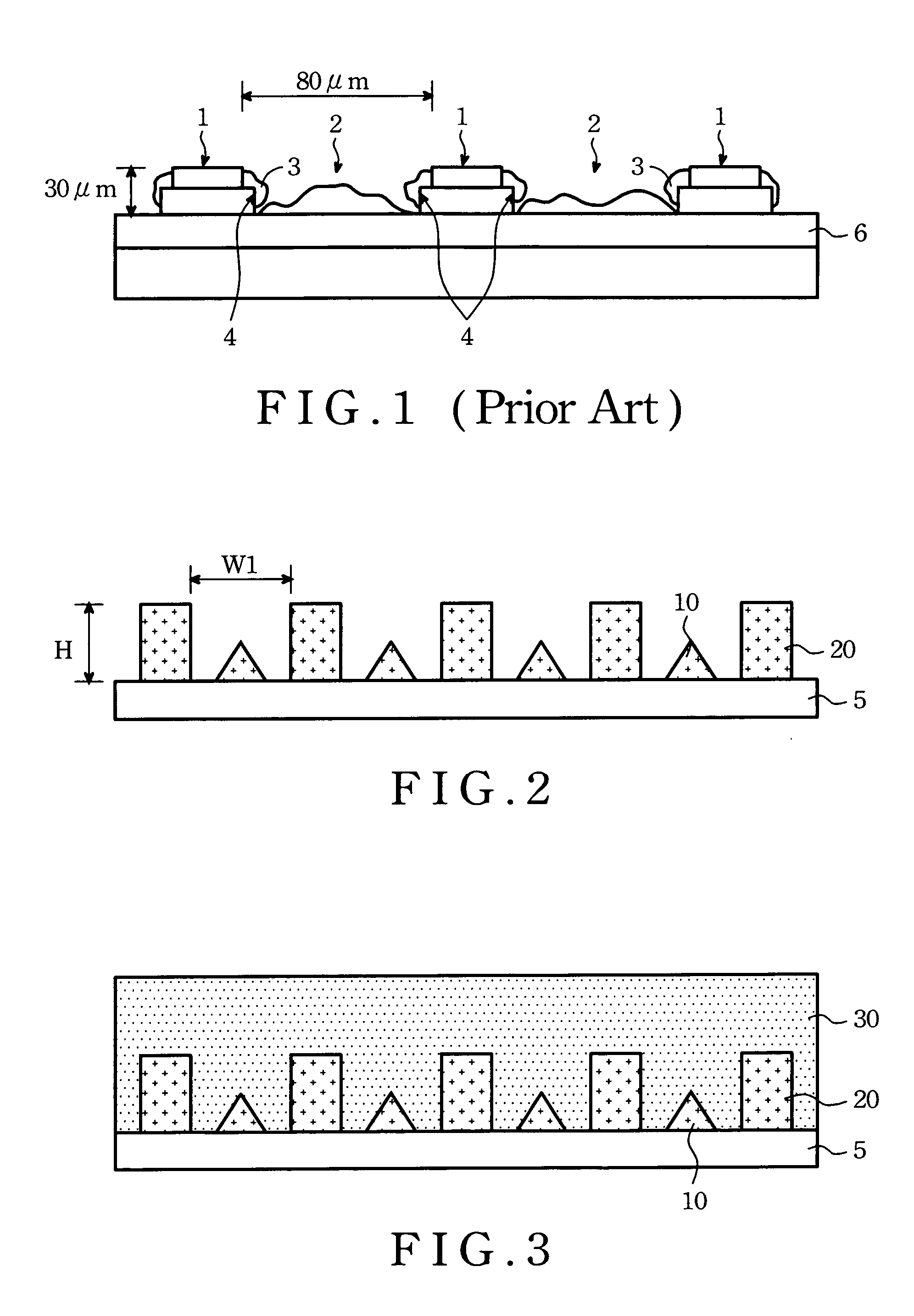
[0021] The conventional fabricating processes for a CNT field emission source formed descried in the background of the invention are usually by a screen print method, which prints a CNT paste layer on cathode lines through openings of the three-electrode structure. Each opening is located at an interval between two gate-lines (vertical lines) having a cathode line (horizontal line) pass through thereto. Since no available mounting points provided in the bottom of the openings for 30 μm in depth of the openings have, the CNT paste is usually adhered to the sidewalls of the openings.

[0022] For a case of using a photosensitive CNT paste layer, the situation is still not being improved due to incomplete exposure on sidewalls during a lithographic process. The present invention can improve above problems. Moreover, the shape and size of the emitting sources can even predetermine.

[0023] The method is described in detailed as follows;

[0024] Firstly, a step of providing an imprint positi...


PUM

PropertyMeasurementUnit
widthaaaaaaaaaa
depthaaaaaaaaaa
diameteraaaaaaaaaa

Abstract

A method of transferring imprint carbon nano-tube (CNT) field emitting source is disclosed. Firstly, cathode lines are screen printed on a substrate. Then a dielectric layer formation on the cathode lines and substrate is followed. Afterward, gate lines formed on the dielectric layer by screen printing are performed. Next a patterning process is carried out to form openings. Subsequently, an imprint negative mold is dipped with CNT paste and imprinted the CNT paste on the cathode lines through the openings. After drawing of pattern from the imprint mold, the CNT paste is cured by annealing. Since the emitting sources are formed through the imprint negative mold, as a result, the size and shape can be predetermined. Moreover, the intervals between gate line and the emitting source are readily control, which resolve the circuit short problem between gate and cathode. Consequently, the current density, brightness, and uniformity of the emitter sources are significantly improved.

Description

FIELD OF THE INVENTION [0001] This invention relates to a field emission display, more particularly to a method of fabricating carbon nanotube (CNT) field emitters by using a method of imprint. By virtue of the imprint mold, both size and shape of emitting source are capable of handling, and the distance between emitting source and gate for three electrodes is easily controlled well. Thus the purpose of lower the driving voltage and cost can be achieved BACKGROUND OF THE INVENTION [0002] Nanotube field emission display comprises an emitting image pixel array formed of conductive paste being screen printed on a substrate having patterned silver cathode thereon. The conductive paste consisting of carbon nanotube (CNT), organic bonding agent, and silver powder. The CNT has a shape of about 5-100 nm in diameter and 1000-3000 nm in length. The principle of field emission is in terms of electric field accelerating cold electrons which are emitted from the tip of each CNT through vacuum sp...

Claims


Application Information

Patent Timeline
Patent Type & Authority Applications(United States)
IPC IPC(8): H01J9/02H01J31/12
CPCB82Y10/00H01J2201/30469H01J31/127H01J9/025
Inventor CHAO, CHING-HSUNSHEU, JYH-RONGCHIANG, LIANG-YUCHANG, YU-YANGLEE, CHENG-CHUNG
Owner IND TECH RES INST
Why Eureka
Try Eureka