

Light emitting apparatus
a technology light emitting tube, which is applied in the direction of lighting and heating apparatus, discharge tube luminescnet screen, semiconductor devices for light sources, etc., can solve the problems of low light emitting efficiency, difficult to adjust the directivity of light emission of small bulbs, and glass bulbs may be cracked, etc., to achieve high light emitting efficiency, easy adjustment of light emission of light emitting apparatus, and easy setting
- Summary
- Abstract
- Description
- Claims
- Application Information
AI Technical Summary
Benefits of technology
Problems solved by technology
Method used
Image

Examples
example 2
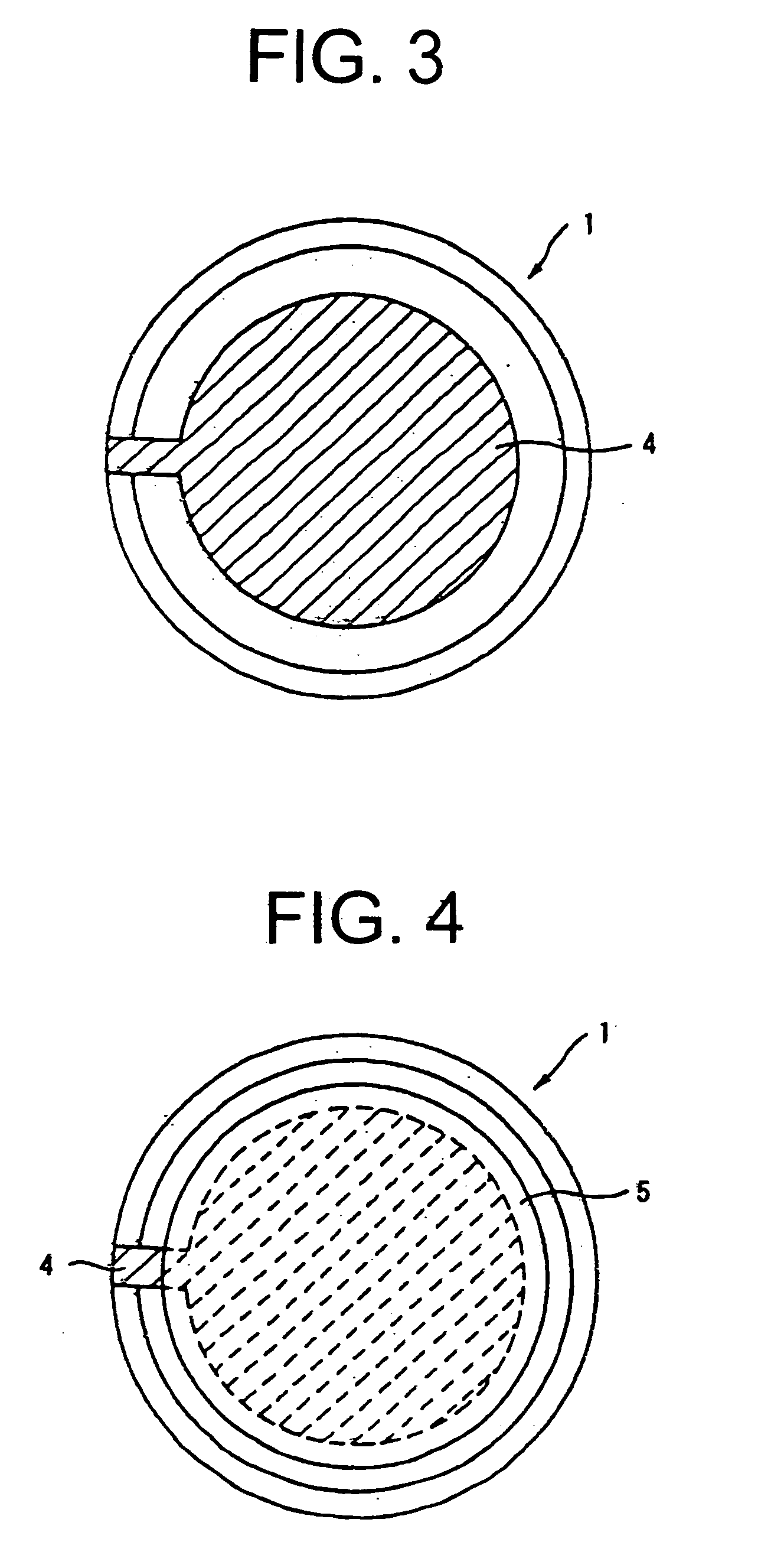
[0256] In the same manner as the example 1, on the inner surface of the warped substrate, the positive electrode layer having a pattern shown in FIG. 3 is formed. An aluminum foil is attached to a portion where is not formed with the light emitting layer in the inner surface of the warped substrate, which has been formed with the positive electrode layer, so that the light emitting layer having a pattern shown in FIG. 4 is formed.
[0257] 1.25 g of o-dichlorobenzene (organic solvent) is dosed with 25 mg of carbonate-based copolymer (hole transporting material), which is used in example 1, 36 mg of PBD (electron transporting material), which is expressed by the following chemical formula, and 0.61 g of coumarin 6 (organic light emitting material), and agitated with a magnetic stirrer; thus an embrocation for forming the light emitting layer is prepared.
[0258] Then, the warped substrate, to which the aluminum foil is attached, is secured on the turntable of the spin coater using a do...
example 3
[0260] The positive electrode layer is formed on the inner surface of the warped substrate in the same manner as the example 1. In a portion of the inner surface of the warped substrate formed with a positive electrode layer, where is not formed with hole transport layer, an aluminum foil is attached so that a hole transport layer having the same pattern as the light emitting layer shown in FIG. 4 is formed. On the inner surface of the warped substrate, which has been attached with the aluminum foil, a thin film of TPD (triphenyldiamine), which is a hole transporting material, is formed by means of vacuum evaporation. The thickness of the hole transport layer is measured using a scanning electron microscope in the same manner as the above. The thickness is 50 nm.
[0261] After that, the light emitting layer and the negative electrode layer are formed in the same manner as the example 1. Thus, on the inner surface of the warped substrate, the electro-luminescent light emitting laminat...
PUM
| Property | Measurement | Unit |
|---|---|---|
| Transmittivity | aaaaa | aaaaa |
| Thickness | aaaaa | aaaaa |
| Electrical conductor | aaaaa | aaaaa |
Abstract
Description
Claims
Application Information