

Multi-chip semiconductor package and fabrication method thereof
- Summary
- Abstract
- Description
- Claims
- Application Information
AI Technical Summary
Benefits of technology
Problems solved by technology
Method used
Image

Examples
Embodiment Construction
[0020] Preferred embodiments for a multi-chip semiconductor package and a fabrication method thereof proposed in the present invention are described in more detail as follows with reference to FIGS. 1A-1F and 2A-2D.
[0021] First Preferred Embodiment
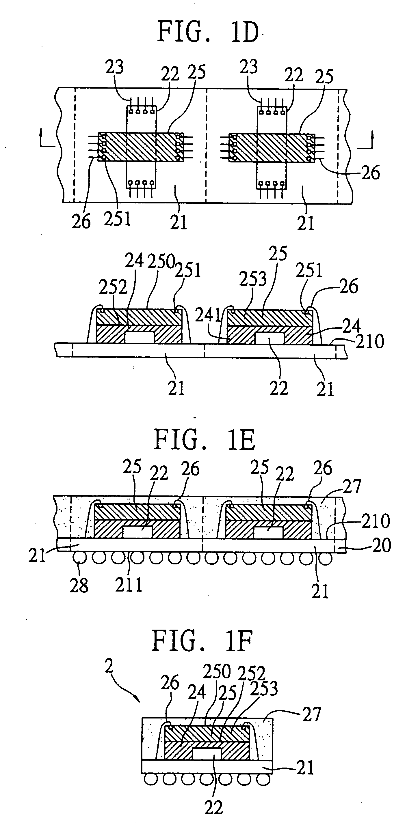
[0022]FIGS. 1A-1F illustrate fabrication processes for a semiconductor package 2 according to a first embodiment of the invention.
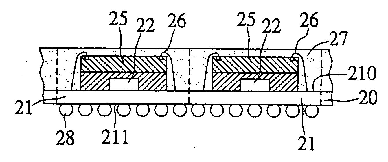
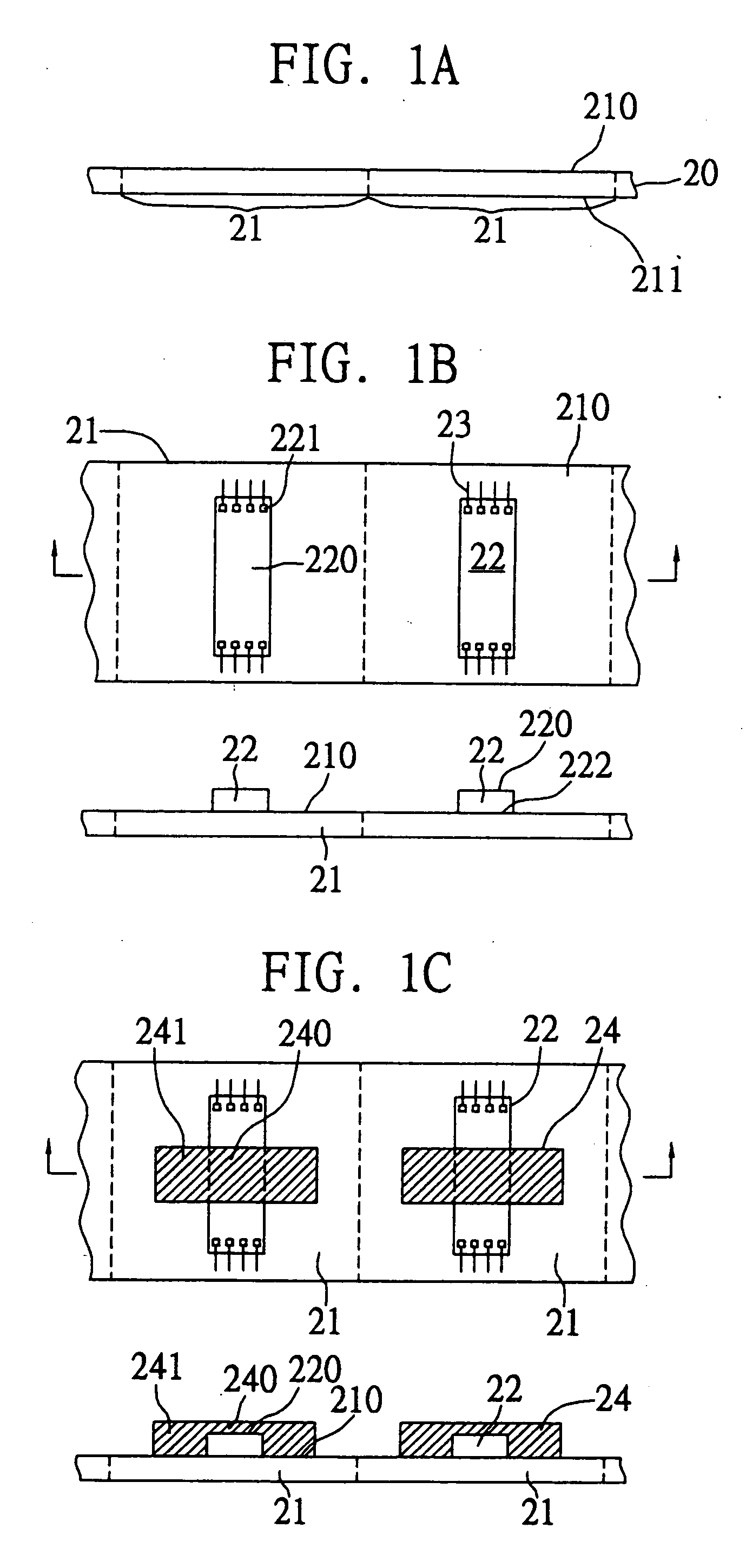
[0023] Referring to FIG. 1A, the first step is to prepare a substrate plate 20 integrally formed of a plurality of substrates 21, which are bordered by dotted lines shown in the drawing. Each of the substrates 21 has an upper surface 210 and a lower surface 211 opposed to the upper surface 210. The substrate plate 20 is primarily made of a conventional resin material, such as epoxy resin, polyimide, BT (bismaleimide triazine) resin, FR-4 resin, etc.
[0024] Referring to FIG. 1B, the next step is to mount at least a first chip 22 on the upper surface 210 of each of the substrates 21. The first chip 22 has an ac...
PUM
 Abstract
Description
Claims
Application Information