Producing method of flexible wired circuit board

a wired circuit board and production method technology, applied in the direction of printed circuit manufacturing, conductive pattern formation, non-metallic protective coating application, etc., can solve the problems substrate is apt to be creased or wrinkled when conveyed using rolls, and elongation, so as to prevent the occurrence of contamination of the flexible wired circuit board obtained

Inactive Publication Date: 2005-03-31
NITTO DENKO CORP
View PDF7 Cites 62 Cited by
  • Summary
  • Abstract
  • Description
  • Claims
  • Application Information

AI Technical Summary

Benefits of technology

[0013] According to the producing method of the flexible wired circuit board of the present invention, even when the electrolysis plating for forming the conductive pattern causes the plated conductive pattern to be larger in thickness at the both end portions thereof than at the widthwise central portion thereof with respect to the widthwise direction of the elongate substrate and in turn causes the elongate substrate to be undulated and deformed plastically at the both widthwise end portions thereof by the wind-up pressure, since the stiffener sheet having a width narrower than the elongate substrate is provided on the elongate substrate, the stif

Problems solved by technology

A thin, elongate, substrate is however apt to be creased or get wrinkled when conveyed using rolls.
When the conductive pattern is formed by the electrolysis plating, the following problems occur with the above-said flexible wired circuit board with the carrier sheet bonded to the elongate substrate, however.
This may in turn cause the problem that in the process subsequent to the conductive pattern

Method used


Image

  • Producing method of flexible wired circuit board
  • Producing method of flexible wired circuit board
  • Producing method of flexible wired circuit board

Examples


example 1

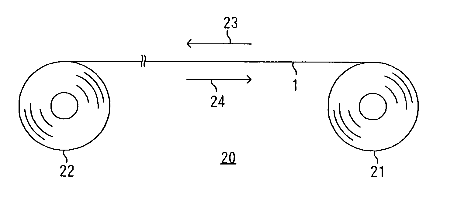
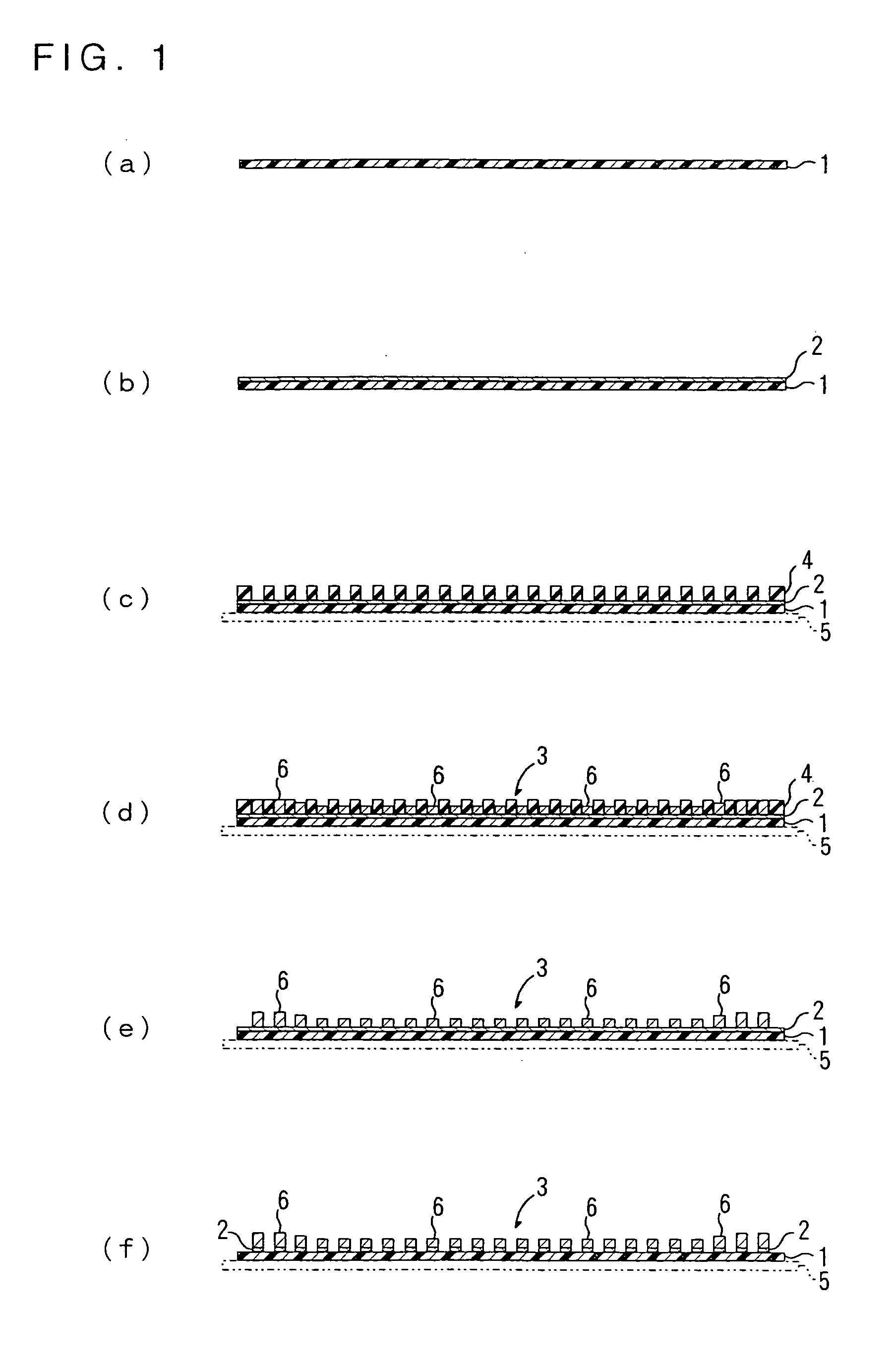
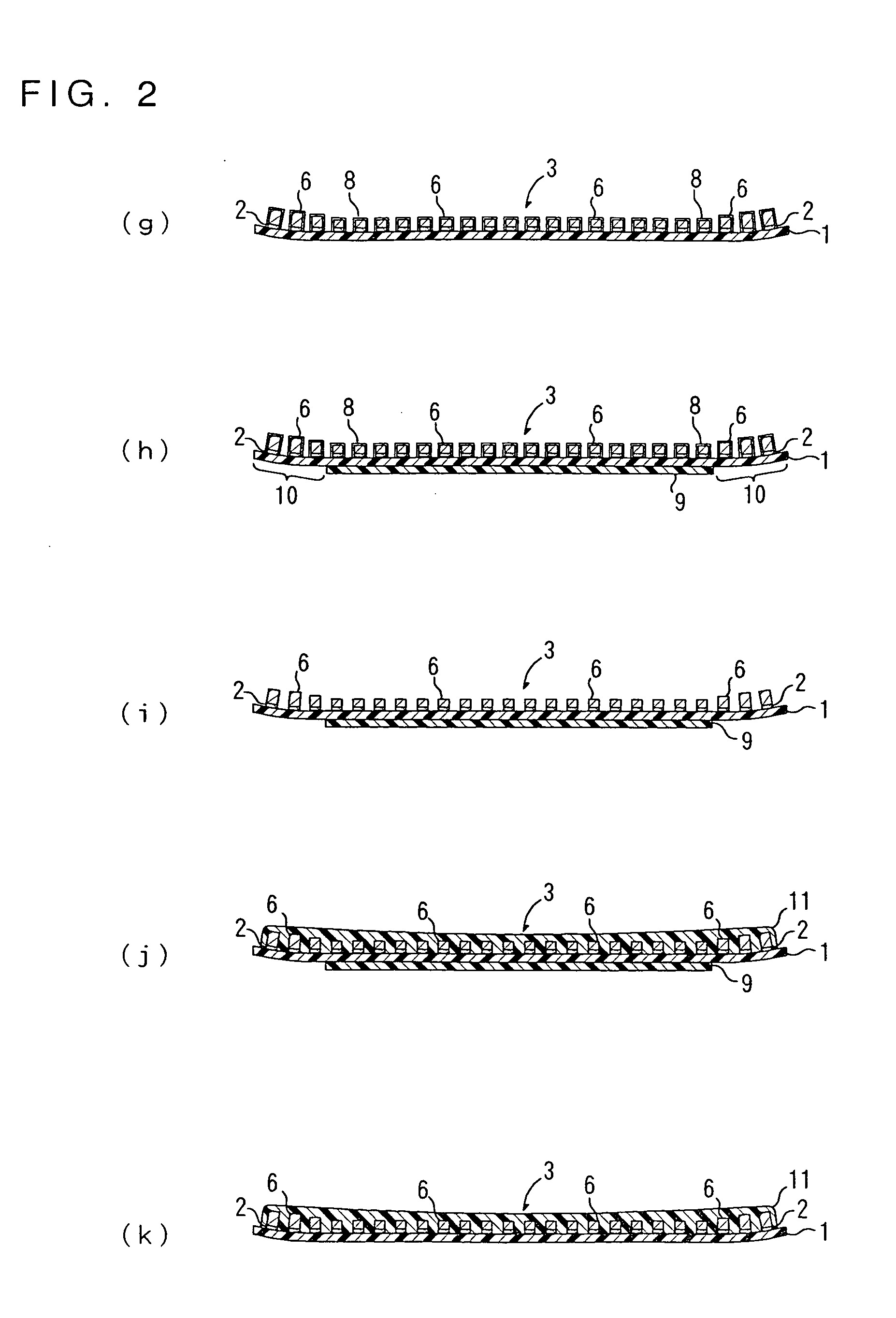
[0061] The delivery and the rewinding was performed between the wind-up roll and the delivery roll were alternately repeated and, in the course of the delivery or the rewinding, the following processes were carried out in sequence.

[0062] An elongate substrate of a polyimide resin sheet having a width of 250 mm and a thickness of 25 μm was prepared (Cf. FIG. 1(a)). Then, a thin metal film comprising a thin chromium film having a thickness of 10 nm and a thin copper film having a thickness of 200 nm was formed on the entire surface of the elongate substrate by the sputtering process (Cf. FIG. 1(b)).

[0063] Then, at the same time as the bonding of a photosensitive dry film resist having a width of 248 mm and a thickness of 19 μm (RY3219 (name of article) available from Hitachi Chemical Co., Ltd.) to a surface of the thin metal film, a stiffener sheet of polyethylene terephthalate resin film with adhesive having a width of 252 mm and a thickness of 50 μm was adhesively bonded to the ba...


PUM

PropertyMeasurementUnit
Thicknessaaaaaaaaaa
Lengthaaaaaaaaaa
Flexibilityaaaaaaaaaa

Abstract

A producing method of a flexible wired circuit board that can prevent the formation of a gap between an elongate substrate and a stiffener sheet bonded thereto to prevent contamination of the flexible wired circuit board obtained. In the process subsequent to the process of forming a conductive pattern 3 on a surface of the elongate substrate 1 by the semi-additive process using electrolysis plating and then annealing the elongate substrate 1 with the conductive pattern 3 in its wound up state, a stiffener sheet 9 having a width narrower than the elongate substrate 1 is bonded to the back side of the elongate substrate 1. Thereafter, an oxidized film formed on a surface of the conductive pattern 3 is removed and then a solder resist 11 is formed thereon. This prevents the strip of the stiffener sheet 9 from the elongate substrate 1 and in turn prevents etching solution or developing solution from entraining in a gap therebetween.

Description

BACKGROUND OF THE INVENTION [0001] 1. Field of the Invention [0002] The present invention relates to a producing method of a flexible wired circuit board and, more particularly, to a method of producing a flexible wired circuit board, while an elongate substrate is conveyed using rolls. [0003] 2. Description of the Prior Art [0004] The method of forming a conductive pattern on a surface of an elongate substrate of a polyimide sheet or the like, while the elongate substrate is conveyed using rolls, for improvement in production efficiency of the flexible wired circuit board, is known. [0005] Along with the trend toward lighter, thinner, and more compact electronic components, the trend in flexible wired circuit boards is also toward thinner profile. A thin, elongate, substrate is however apt to be creased or get wrinkled when conveyed using rolls. To prevent this, for example JP Laid-open (Unexamined) Patent Publication No. Hei 6-132628 proposes that a carrier film, such as a polyeth...

Claims


Application Information

Patent Timeline
IPC IPC(8): H05K1/00H05K3/28H05K1/02H05K3/00H05K3/06H05K3/10H05K3/18H05K3/22
CPCH05K1/0393H05K3/007H05K3/0097H05K2203/1545H05K3/28H05K2203/0156H05K3/108H05K3/22H05K3/06
Inventor NAITO, TOSHIKISHINOGI, YOSHIFUMIYAMATO, TAKESHI
Owner NITTO DENKO CORP
Why Eureka
Try Eureka