Microelectromechanical system and method for fabricating the same

a micro-electromechanical and manufacturing method technology, applied in the direction of instruments, radiation controlled devices, and the details of the semiconductor/solid-state device, can solve the problems of controller damage, controller deterioration, controller damage, etc., and achieve good transducer performance and reduce wiring resistance

Inactive Publication Date: 2005-03-31
PANASONIC CORP
View PDF2 Cites 65 Cited by
  • Summary
  • Abstract
  • Description
  • Claims
  • Application Information

AI Technical Summary

Benefits of technology

[0018] In order to overcome the problems described above, an object of the present invention is to provide a micro-electromechanical system, which prevents the interconnects from being damaged even at a high temperature, ensures good transducer performance, and reduces the wiring resistance, and a method for fabricating such a system.

Problems solved by technology

Accordingly, if the process step of forming the transducer must be carried out at an elevated temperature, then the controller may deteriorate due to the heat, which is a problem.
Meanwhile, the controller of a normal CMOS circuit has a thermal resistance of at most about 450° C. to about 525° C. Accordingly, if the transducer, requiring such a high-temperature process, were formed after the controller has been provided, then the controller might be damaged.
It is known that the controller is damaged mainly because an aluminum alloy, which is usually used in the interconnect portion thereof, increases its resistance so much as to be disconnected.
In addition, even at a temperature lower than 660° C., aluminum is likely to create voids due to grain growth or atomic diffusion.
Thus, if the interconnects of the controller are made of aluminum with such a low melting point, then the interconnects would deteriorate while the transducer is being fabricated.
Accordingly, the loss and resistance variation of a long interconnect are particularly significant.
However, when the barrier layer is thin, most of the atoms in the barrier layer are subject to interfacial effects produced between the barrier layer and the insulating film, and therefore, tend to have decreased grain sizes and randomized crystal directions.
Thus, this technique does not contribute effectively to achieving a lower resistance than that of aluminum.
In addition, the portions of the silicon substrate to be etched away cannot be fixed definitely.
Consequently, it is difficult to prevent the controller from being damaged by over-etching or the transducer from losing its reliability due to under-etching.

Method used


Image

  • Microelectromechanical system and method for fabricating the same
  • Microelectromechanical system and method for fabricating the same
  • Microelectromechanical system and method for fabricating the same

Examples


Embodiment Construction

[0057] Hereinafter, preferred embodiments of the present invention will be described with reference to the accompanying drawings.

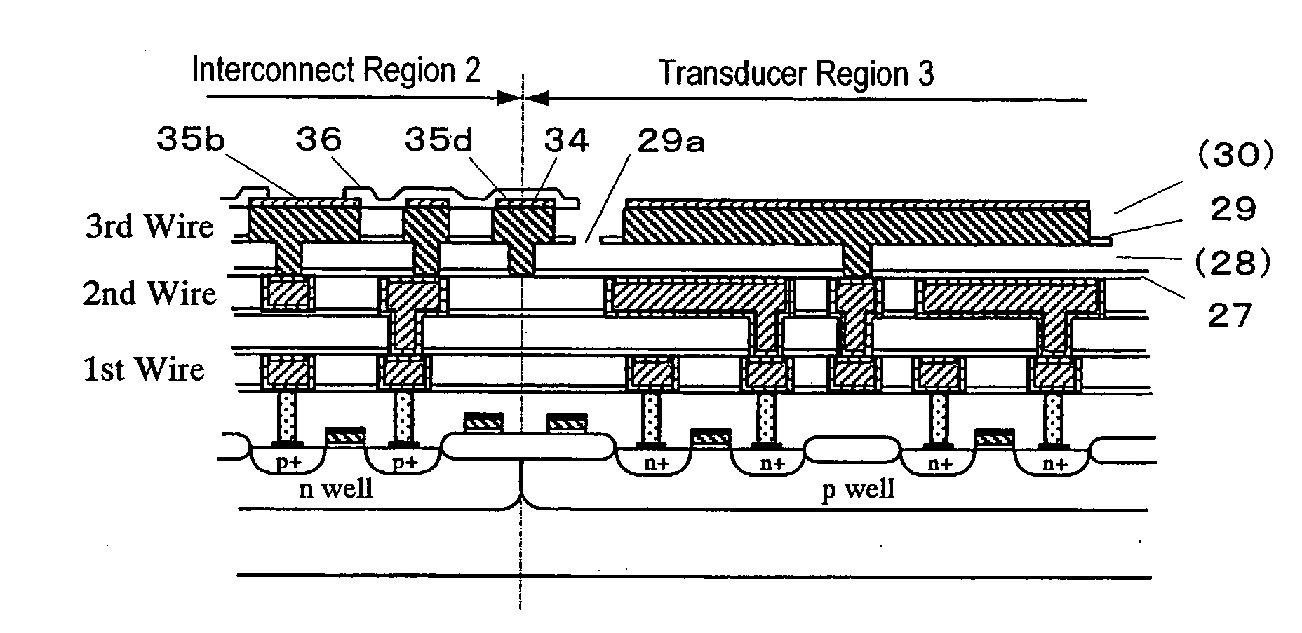
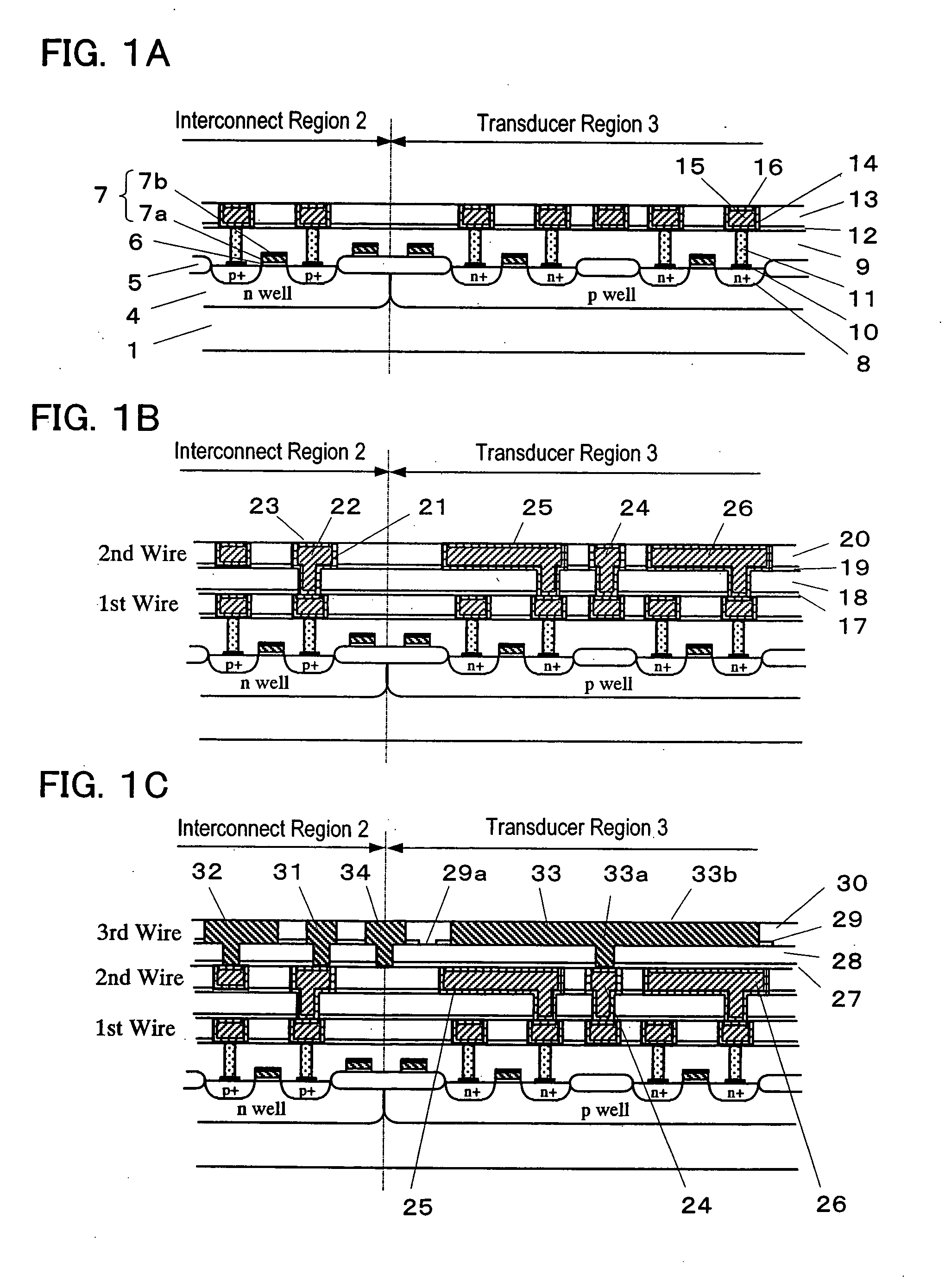
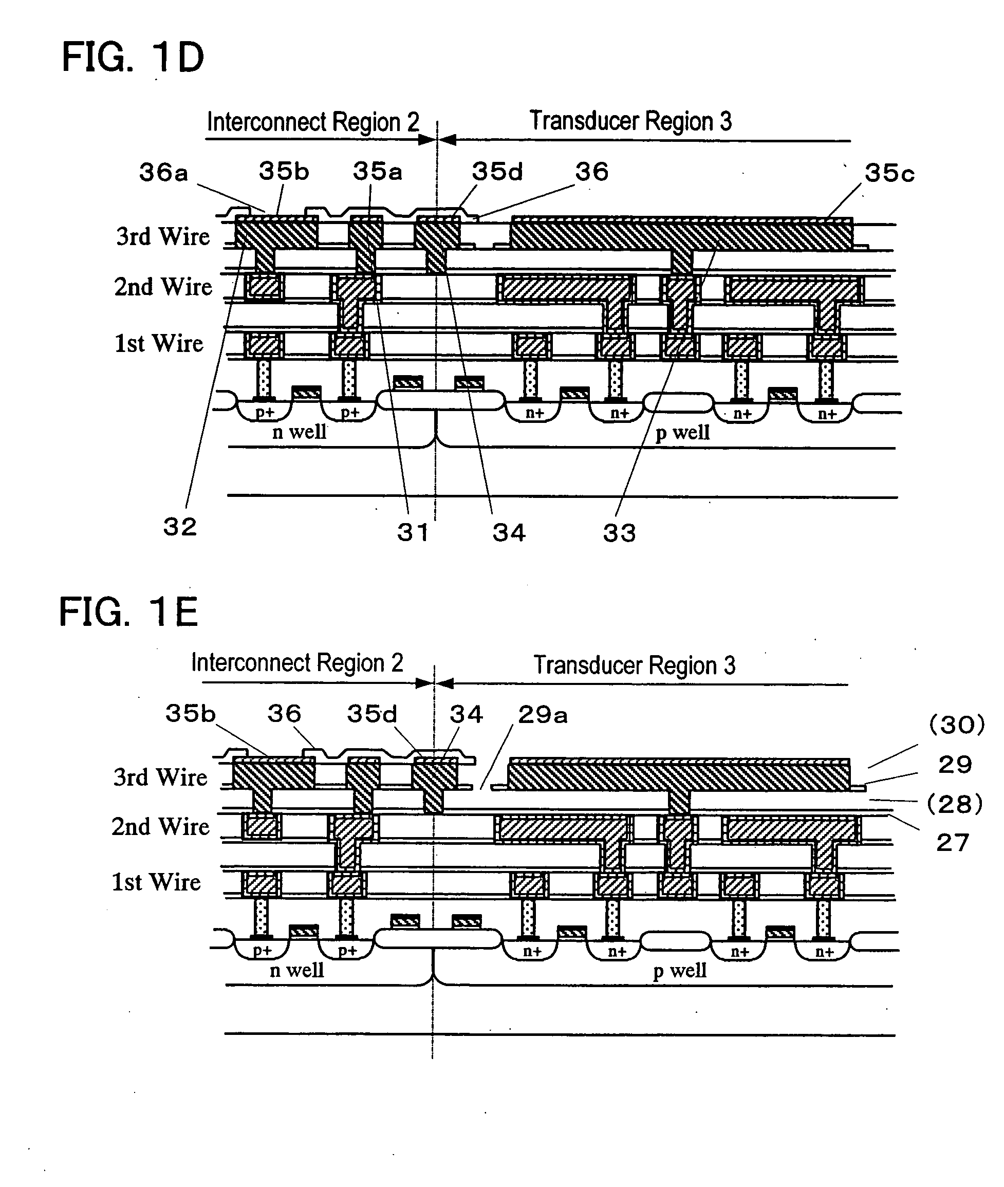
[0058] First, referring to FIGS. 1A, 1B and 1C, illustrated are partially enlarged cross-sectional views of the substrate during the first half of a manufacturing process according to this preferred embodiment.

[0059] Specifically, FIG. 1A shows a cross section of the substrate on which the process step of forming the first conductor layer has just been carried out. The substrate for use in this preferred embodiment is an n-type silicon wafer 1, on which an interconnect region 2 and a transducer region 3 will be defined.

[0060] In the interconnect region 2, a CMOS circuit or a BiCMOS circuit has preferably been provided so as to generate a drive signal for driving a transducer in response to an external input signal. In the transducer region 3 on the other hand, a plurality of transducers and a plurality of switching elements for selecting transducers to ...


PUM

PropertyMeasurementUnit
thicknessaaaaaaaaaa
temperatureaaaaaaaaaa

Abstract

A microelectromechanical system includes a substrate, a transducer supported on the substrate and a conductor layer, which is also supported on the substrate and electrically connected to the transducer. The transducer includes a portion made of silicon or a silicon compound. The conductor layer is made of a refractory conductor, which includes, as its main ingredient, at least one element selected from the group consisting of copper, gold and silver. At least a portion of the conductor layer is located at an intermediate level between the silicon or silicon compound portion of the transducer and the substrate.

Description

BACKGROUND OF THE INVENTION [0001] 1. Field of the Invention [0002] The present invention relates to a micro-electromechanical system, in which a transducer and an interconnect portion for electrically connecting the transducer to an external device are integrated together on the same substrate, and also relates to a method for fabricating such a system. [0003] 2. Description of the Related Art [0004] Microelectromechanical systems (MEMS), including a transducer and a controller that are integrated together on the same substrate, have recently been researched and developed extensively. As used herein, the “transducer” means an element having the function of converting electrical energy into energy in another form and / or vice versa. A micro actuator and a micro sensor, at least part of which is a physically deformable structure, are typical transducers for converting electrical energy into mechanical energy. [0005] A MEMS of that type is fabricated by providing a controller on a subs...

Claims


Application Information

Patent Timeline
Patent Type & Authority Applications(United States)
IPC IPC(8): B81B7/00H01L21/768H01L21/8238H01L23/532H01L27/06
CPCB81B7/0006B81B7/0012H01L21/76838H01L21/76846H01L21/76849H01L21/823871H01L23/53233H01L2924/0002H01L23/53238H01L27/0617B81C1/00246H01L2924/00H01L21/7682H01L23/53271
Inventor MUSHIKA, YOSHIHIRO
Owner PANASONIC CORP
Why Eureka
Try Eureka