Liquid crystal display device

a technology of liquid crystal display and display device, which is applied in the direction of identification means, lighting and heating apparatus, instruments, etc., can solve the problems of power consumption, difficult to oppose precisely directly the entrance surface b>4/b>a of the light guide b>4/b>, and complicated assembling process

Inactive Publication Date: 2005-03-31
PANASONIC LIQUID CRYSTAL DISPLAY CO LTD +1
View PDF6 Cites 14 Cited by
  • Summary
  • Abstract
  • Description
  • Claims
  • Application Information

AI Technical Summary

Benefits of technology

[0035] According to the construction described in (11) to (13), by bringing the plurality of light-emitting elements into abutment with positioning shapes specially provided on the inner peripheries of the respective through-holes or the respective through-holes, the positions of the light-emitting elements relative to the entrance surface of the light guide are restricted, whereby the distance between the light-emitting elements and the entrance surface of the light guide can be maintained at a design value and the occurrence of luminance irregularity on the display screen of the liquid crystal display panel can be restrained.

Problems solved by technology

However, many mobile telephones and small-sized mobile information terminals (such as PDAs) use solid-state light-emitting elements such as light-emitting diodes (LEDs) with low power consumption.
In addition, the light-emitting parts and the entrance surface 4A of the light guide 4 are difficult to oppose precisely directly.
This has been one problem to be solved in the related art.
Moreover, because of the structure in which the LEDs 8 are mounted in the molded case 6, wiring means is needed for connecting power supply lines for the LEDs 8 to power source terminals (or power source electrodes) of driver circuits mounted on a printed circuit board (not shown), so that the assembling process becomes complicated.
Accordingly, a folding process is needed, so that work efficiency lowers and cracks or the like may occur in a folded portion, incurring malfunction.
In addition, the thickness of the auxiliary illuminating device increases, with the result that this increase of the thickness hinders a further reduction in the entire thickness of a liquid crystal display device in which such an auxiliary illuminating device is incorporated, and hence a further reduction in the thickness of a terminal using such a liquid crystal display device.
These limitations are also a cause which hinders a further reduction in the thickness of the auxiliary illuminating device as well as a further reduction in the thickness of the entire terminal in which the auxiliary illuminating device is incorporated.

Method used


Image

  • Liquid crystal display device
  • Liquid crystal display device
  • Liquid crystal display device

Examples


first embodiment

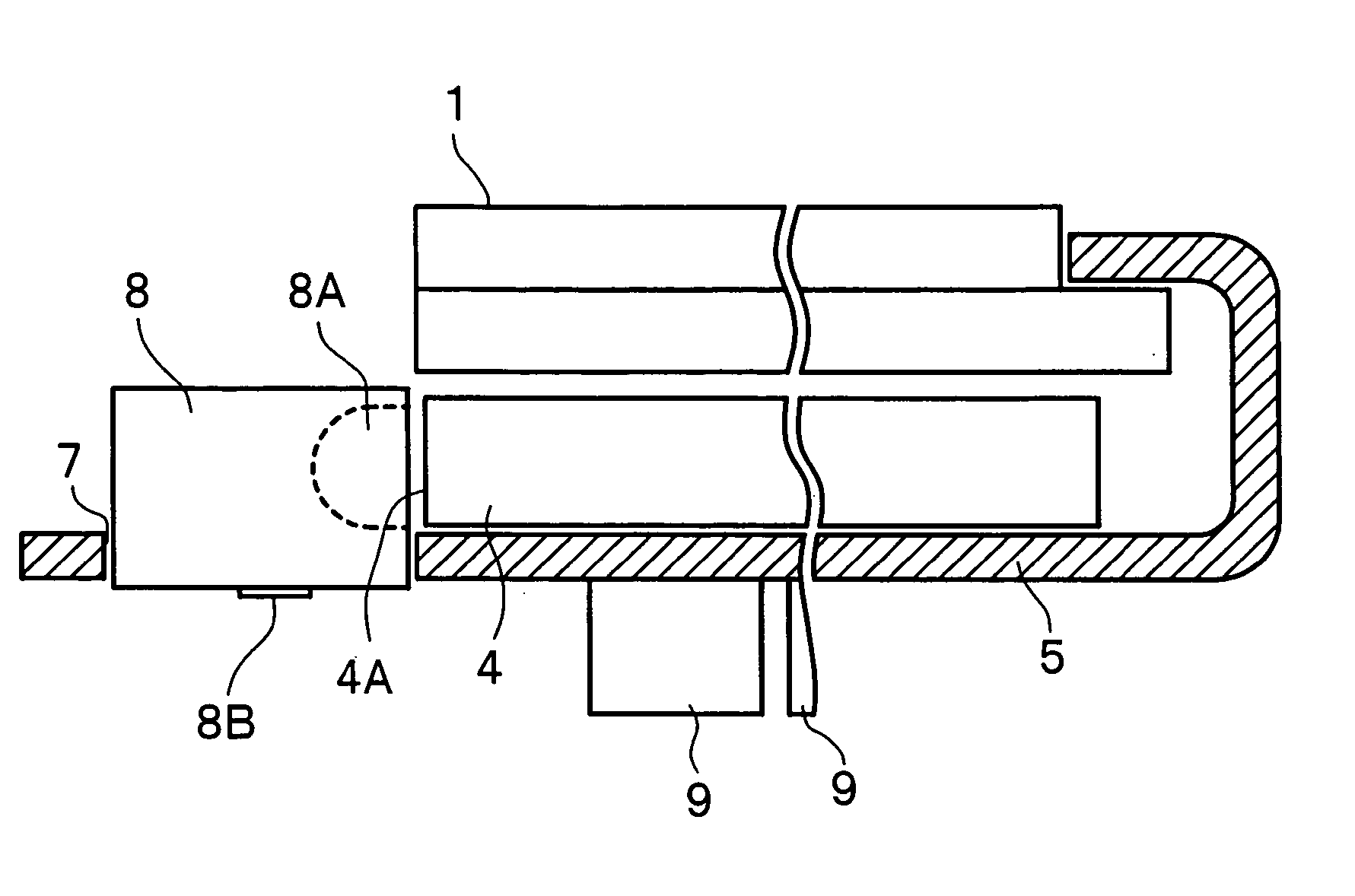
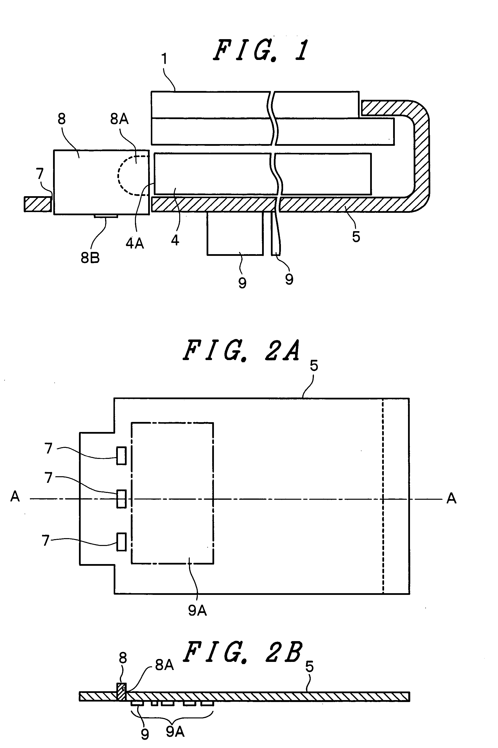
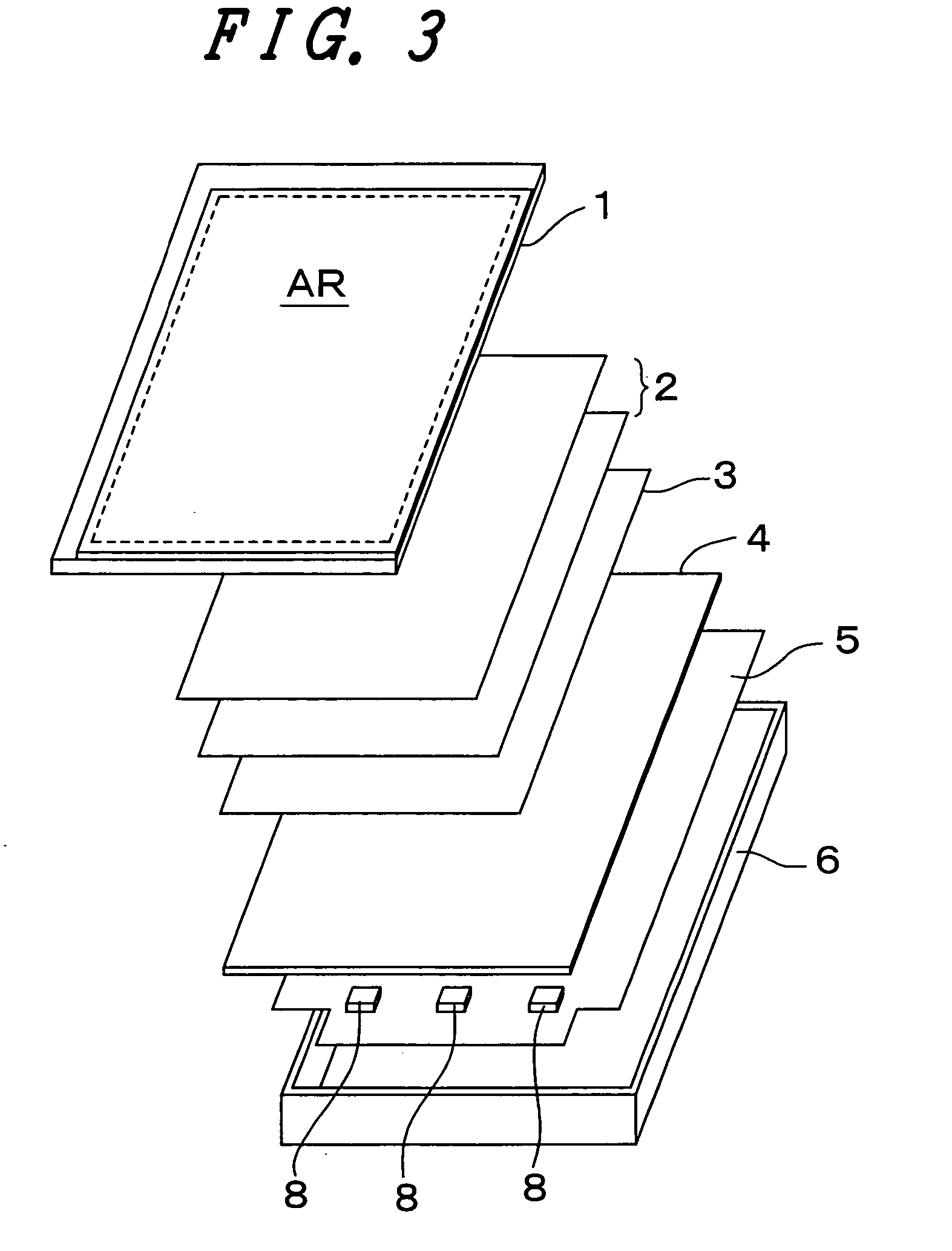
[0056] The LEDs 8 are mounted in the state of being respectively inserted through through-holes 7 formed in a printed circuit board 5. This printed circuit board 5 is a flexible printed circuit board. The printed circuit board 5 of the first embodiment is folded toward the liquid crystal display panel 1 at an end portion opposite to the side where the LEDs 8 are mounted, and is connected to an electrode terminal led out of either one of the substrates of the liquid crystal display panel 1. Incidentally, at an end portion where the LEDs 8 are mounted or an end portion adjacent to the end where the LEDs 8 are mounted, the printed circuit board 5 may be folded and connected to a terminal of the liquid crystal display panel 1.

[0057] In a light-emitting portion 8A of each of the LEDs 8, in terms of the efficiency of utilization of light, it is desirable that the size of the light-emitting portion 8A taken in the thickness direction of the light guide 4 be made not greater than the thickn...

second embodiment

[0064] as to the printed circuit board 5 on which the LEDs 8 are mounted from the same side together with the other electronic components 9, the light-emitting portions 8A of the respective LEDs 8 can be disposed to be accurately directly opposed to the entrance surface 4A of the light guide 4 without the need to fold the printed circuit board 5 in the portion of the LEDs 8, thereby enabling a reduction in the number of process steps.

[0065]FIGS. 5A to 5C are explanatory views of the advantage of the mounting structure of the LEDs on the printed circuit board which constitutes the auxiliary illuminating device in the liquid crystal display device according to the invention. FIG. 5A is a schematic plan view showing for comparison purposes a case in which a printed circuit board does not have mounting through-holes for LEDs, while FIGS. 5B and 5C are schematic plan views showing different cases in each of which a printed circuit board has mounting through-holes for LEDs. Incidentally,...


PUM

PropertyMeasurementUnit
sizeaaaaaaaaaa
sizeaaaaaaaaaa
heightaaaaaaaaaa

Abstract

Light-emitting elements can be accurately directly opposed to the entrance surface of a light guide at an accurate distance therefrom, and can be mounted on a single side of a printed circuit board together with other electronic components, whereby the number of manufacturing steps and the thickness of a liquid crystal display device can be reduced. The light guide and the printed circuit board are disposed on the back surface of the liquid crystal display panel, and the respective light-emitting elements are inserted through through-holes formed to extend through the printed circuit board, with the light-emitting portions of the respective light-emitting elements opposed to the entrance surface of the light guide. The light-emitting elements, together with the other electronic components, are mounted on the printed circuit board from one side. Electrodes of the light-emitting elements are bridged and secured to a mounting surface of the printed circuit board.

Description

BACKGROUND OF THE INVENTION [0001] The present invention relates to a liquid crystal display device and, more particularly, to a liquid crystal display device which is provided with an auxiliary light source device having a light guide with solid-state light-emitting elements such as light-emitting diodes disposed at a side edge of the light guide as a light source. [0002] In small-sized information terminals such as mobile telephones or mobile information terminals, it is general practice to adopt, as their display devices, liquid crystal display devices which are energy efficient, small-sized and light weight. The liquid crystal display devices are classified into two types: one type in which external light is utilized as illuminating means for visualizing an electronic latent image formed on a liquid crystal display panel; and the other type in which an auxiliary illuminating device is disposed on the back or front surface of a liquid crystal display panel. The auxiliary illumina...

Claims


Application Information

Patent Timeline
Patent Type & Authority Applications(United States)
IPC IPC(8): F21V8/00F21Y101/02G02F1/13357G02F1/1345G09F9/00H05K1/18
CPCG02B6/0083G02F1/133603G02F1/133615H05K2201/10106H05K1/181H05K1/182H05K1/0274G02F1/1335
Inventor AOYAGI, MASAYUKIMORIKA, YASUSHI
Owner PANASONIC LIQUID CRYSTAL DISPLAY CO LTD
Why Eureka
Try Eureka