In particular, while
processing in an area where the patterns having the same dimension are arranged with a uniform density can be made with relative ease, it is generally extremely difficult to make
processing with sufficient precision in an area where the patterns have low uniformity.
However, in reality, some of the exposing light reaches the area on the semiconductor substrate where the patterned
mask is provided, due to scattering of the exposing light passing through the space between the
mask patterns.
With the decrease of the pattern dimension, such unintended
exposure of the
resist layer becomes a significant problem.
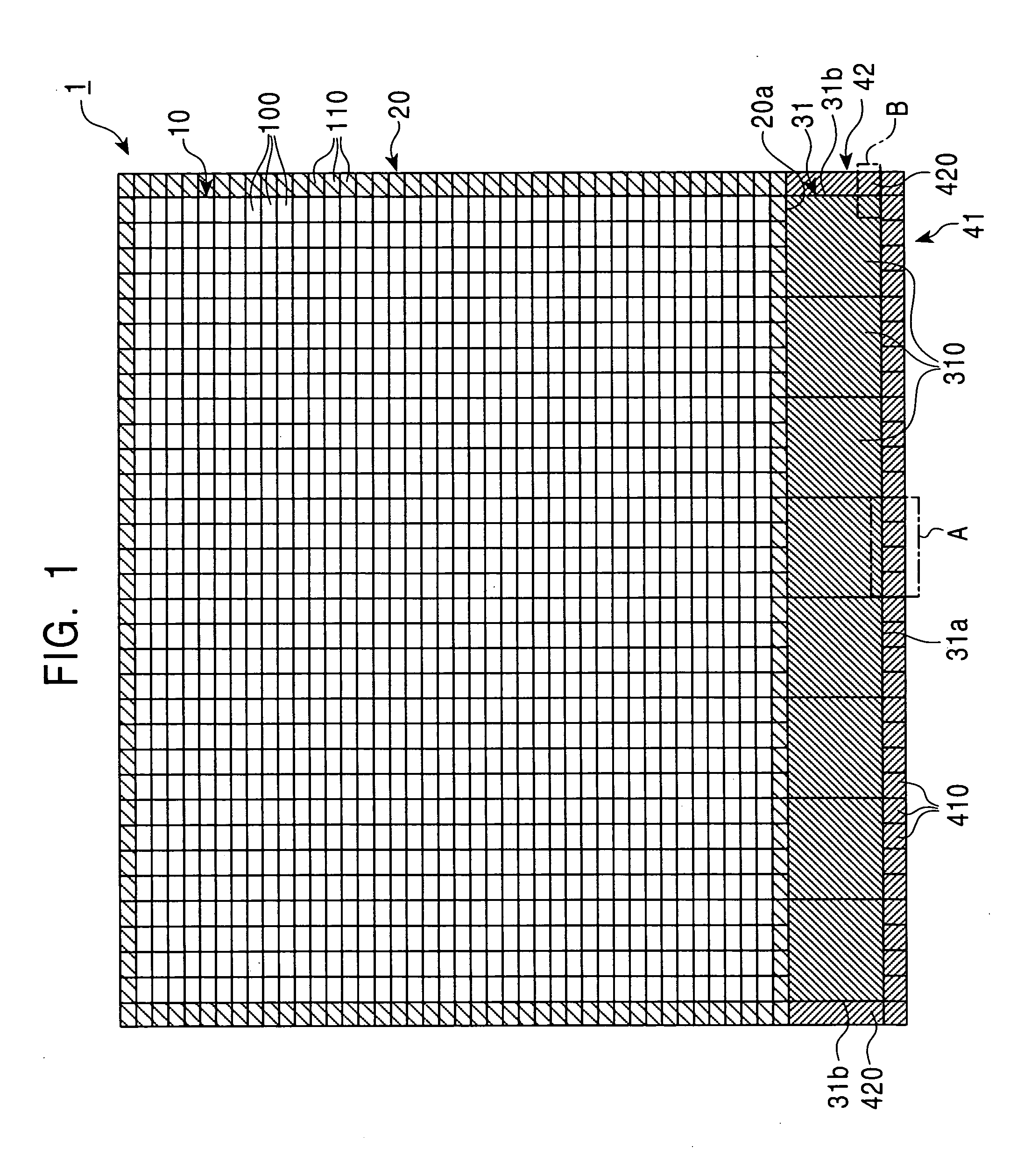
However, at the outermost portion of the memory
cell array, the pattern regularity is lost and the uniformity of pattern density is markedly degraded.
As a result, the
processing at the outermost portion of the memory cell array often leads to an insufficient precision.
However, according to the technique disclosed in
Patent Document 1, no measure is provided for improving the uniformity of pattern density in the peripheral circuit region, leading to marked irregularities in the pattern density at the perimeter of the peripheral circuit region, thus often resulting in
pattern formation with insufficient precision.
Therefore, a simple application of the technique disclosed in
Patent Document 1, i.e., arranging dummy cells each having the same device pattern as with the peripheral circuit cell around the perimeter of the peripheral circuit region, would require an excessively large waste of the area on the
chip.
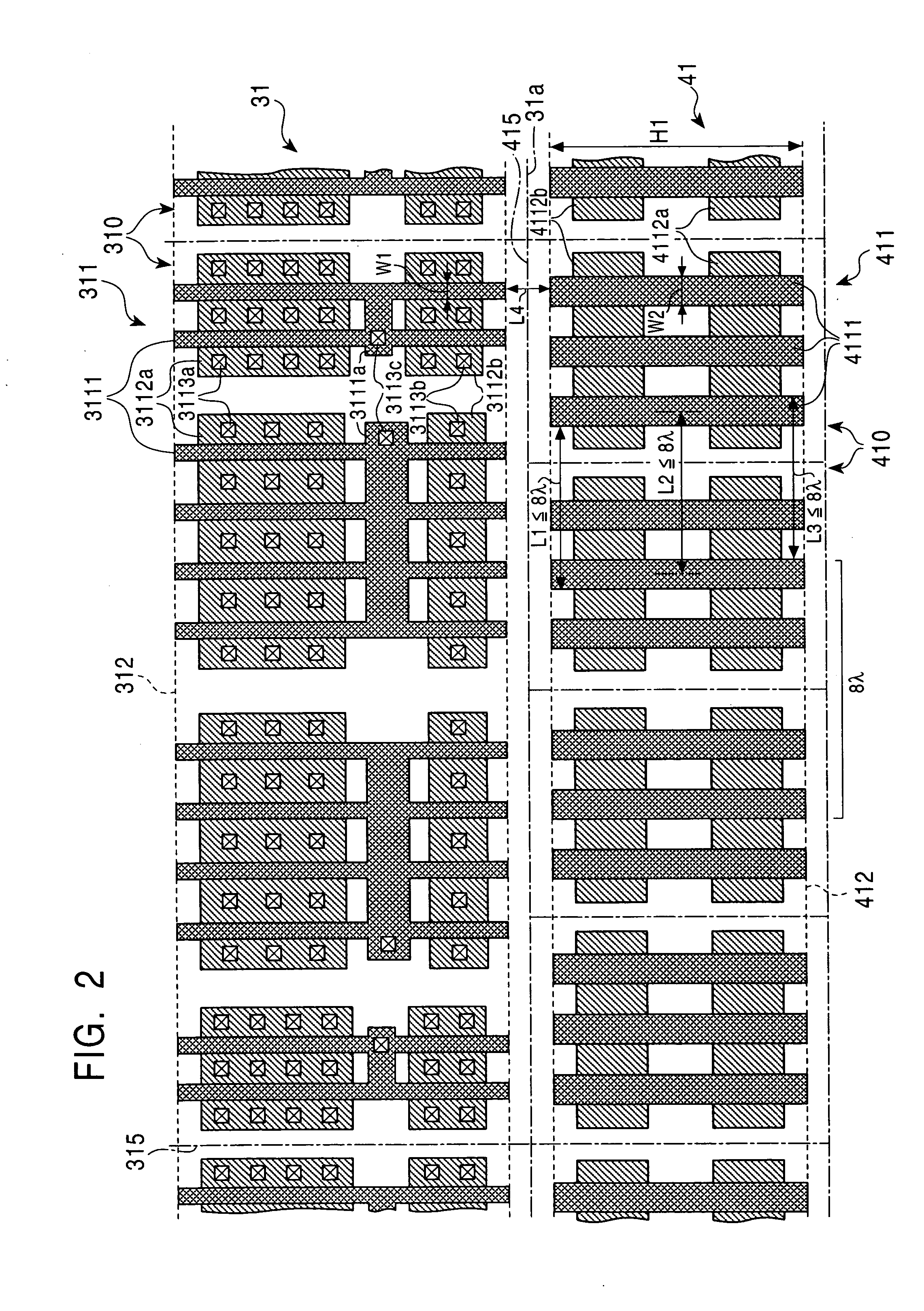
This procedure leads to the creation of gaps between the device patterns and the dummy cells.
With such a layout, while the uniformity of the pattern density is improved compared to a layout having no dummy patterns, the uniformity is not sufficiently improved for advanced fine-patterning technology.
Such dummy pattern would not provide the pattern regularity of the same level of regularity at the internal portion of the peripheral circuit region.
Accordingly, even if the dummy pattern layout technique disclosed in
Patent Document 2 improves the uniformity of pattern density, this technique does not improve the pattern regularity.
Accordingly, even if the dummy pattern arranging technique disclosed in Patent Document 2 is applied to the peripheral circuit region, significant pattern deformations would occur at the outermost portion of the peripheral circuit region due to poor uniformity of pattern density and poor pattern regularity.
Thus, it becomes difficult to perform processing with the high precision required for advanced fine-patterning technology in the future.
However, such extensive correction generally leads to a reduction of process margin, that is, the
resist pattern becomes susceptible to significant dimensional deviation due to deviation in the exposing
light intensity, the deviation of the focus, and the like, over the exposed area.
As a result, the
resist pattern is formed with
extremely poor precision around the perimeter of the peripheral circuit region.
Furthermore, with the technique disclosed in Patent Document 2, logical synthesis processing, which requires a great deal of calculation, is required, leading to a long processing time for the layout design.

