Variable rotational assignment of interconnect levels in integrated circuit fabrication

a technology of interconnect level and rotational assignment, which is applied in the direction of originals for photomechanical treatment, instruments, and semiconductor/solid-state device details, etc., can solve the problems of increasing the database size associated with extraction, increasing the write time, and removing techniques previously realized, etc., and achieves the effect of finer granularity

Inactive Publication Date: 2005-04-14
LUCENT TECH INC
View PDF0 Cites 2 Cited by
  • Summary
  • Abstract
  • Description
  • Claims
  • Application Information

AI Technical Summary

Benefits of technology

The present invention provides methods and apparatus for use in the fabrication of integrated circuits wherein non-horizontal and non-vertical wires or interconnect lines, i.e., non-0° and non-90° wires, respectively, are assigned to interconnect mask layers or levels separate from mask layers having horizontal and vertical wires assigned thereto. The assigned non-horizontal and non-vertical interconnect lines are then rotated to a horizontal and / or vertical orientation for printing the mask layers in which they are located. Assignment and rotation may take place within a CAD system. All mask layers may then be printed without the above-described litho step problem. Then, at the time of exposure of the appropriate metal layers of the integrated circuit, the masks associated with the non-horizontal and non-vertical wires are rotated so that the wires thereon are returned to their original non-horizontal and non-vertical orientation. The metal layers are then exposed. With the use of variable rotational assignment according to the invention and thus the elimination of the litho step problem, non-horizontal and non-vertical wires can traverse the entire chip surface, rather than just the corners as in the conventional Manhattan geometry, while interconnecting circuit points and saving on interconnect distances.
Advantageously, the present invention eliminates various problems associated with conventional IC fabrication techniques and allows for interconnect distances to be reduced over, for example, a Manhattan interconnect by as much as 30%. Furthermore, the capacitance interaction of interconnects on lower and higher levels can be made less influential by using this invention, which from a noise coupling perspective is highly advantageous. Since the lower and upper layers are not parallel, the coupling capacitance to these interconnects will extend for only a fraction of the wire's length. Since this wire will be crossing other wires, the capacitive interaction of these other wires can cancel the capacitance of this wire, thus allowing lower noise due to this coupling effect.
This allows for finer granularity in the placement of the interconnect.

Problems solved by technology

This causes several problems.
Second, the extraction of this wire causes problems since the W and L are not well-defined, as illustrated by the waviness of the lines in FIG. 2.
When this wire is a poly silicon gate, the extraction in a transistor causes most Computer Aided Design or CAD tools to give fictitious results, as well as increase the database size associated with the extraction.
Unfortunately, several problems have prevented this technique from being previously realized.
For example, the three problems described above are impediments to the use of such a technique.
But, as explained above, if this is done: (1) write time will increase enormously; (2) CAD extraction will be a problem; and (3) the data storage and file size will be large.

Method used


Image

  • Variable rotational assignment of interconnect levels in integrated circuit fabrication
  • Variable rotational assignment of interconnect levels in integrated circuit fabrication
  • Variable rotational assignment of interconnect levels in integrated circuit fabrication

Examples


Embodiment Construction

The present invention will be explained below in the context of an illustrative embodiment employing non-horizontal / non-vertical interconnect wires formed at angles of 45° and / or multiples thereof. However, it is to be understood that the present invention is not so limited. Rather, as will be 25 explained below, the methodologies of the invention may be more generally applied in order to form non-horizontal / non-vertical interconnect wires at various other angles.

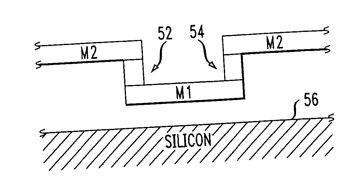
An illustrative embodiment of the invention will now be explained. Instead of printing a 45° line in a Manhattan type geometry, the methodology of the present invention provides for assigning 45° lines to a particular layer of the IC being fabricated, for example, the Metal 2 layer (M2). The horizontal and vertical lines are assigned to another layer, for example, the Metal 1 layer (M1). The M2 layer therefore contains the 45° and / or 45° and 135° interconnects used in the formation of the IC. However, at the time the mas...


PUM

PropertyMeasurementUnit
angleaaaaaaaaaa
distancesaaaaaaaaaa
sizeaaaaaaaaaa

Abstract

Integrated circuit fabrication techniques are provided which allow non-horizontal / non-vertical wires to traverse the entire chip surface, rather than just the comers as in the conventional Manhattan geometry, while interconnecting circuit points. This is achieved by employing a variable rotational assignment methodology with respect to the interconnect layers or levels during the IC fabrication operation. These techniques thus eliminate the litho step problem, reduce interconnect distances and lessen the influence of capacitance interaction between interconnect wires.

Description

FIELD OF THE INVENTION The invention relates to integrated circuit fabrication and, more particularly, to methods and apparatus for performing variable rotational assignment of interconnect levels for use in the fabrication of integrated circuits. BACKGROUND OF THE INVENTION It is known that conventional integrated circuit (IC) fabrication processes utilize a so-called “Manhattan geometry” to form the circuits and interconnects associated with an IC. In such a geometry, horizontal and vertical wires formed at 90° (degrees) to one another are used to connect points across the IC or chip, while a 45° wire is typically used in corners of the chip and, in some cases, in the internal section or interconnect, so that distances can be reduced. However, in order to implement these wires or edges in a Manhattan IC, one must adhere to the so-called “litho step.” The litho step is defined as the resolution movement allowed in the x or y direction. For example, in 0.35 μm (micrometers), 0.25 ...

Claims


Application Information

Patent Timeline
Patent Type & Authority Applications(United States)
IPC IPC(8): G03F1/08G06F17/50H01L21/027H01L21/3205H01L21/768H01L21/82H01L23/52H01L23/528
CPCH01L21/76838H01L23/528H01L2924/0002H01L2924/00
Inventor GABARA, THADDEUS JOHNJOMAA, TAREK CHAKER
Owner LUCENT TECH INC
Why Eureka
Try Eureka