MEMS based contact conductivity electrostatic chuck

a contact conductivity and electrostatic chuck technology, applied in the direction of semiconductor devices, electrical equipment, semiconductor/solid-state device testing/measurement, etc., can solve the problems of costly power supply and consumption considerations, deleterious effects on the wafer, so as to improve process control and efficiently clamp the substrate

Inactive Publication Date: 2005-04-14
AXCELIS TECHNOLOGIES
View PDF5 Cites 26 Cited by
  • Summary
  • Abstract
  • Description
  • Claims
  • Application Information

AI Technical Summary

Benefits of technology

[0012] The present invention is generally directed to a multi-polar electrostatic chuck and method for cooling or heating a semiconductor substrate. The multi-polar electrostatic chuck, for example, comprises a clamping plate that is operable to efficiently clamp the substrate thereto, and to cool or heat the substrate in a generally uniform manner thereacross, thereby improving process control. According to one example, the clamping plate comprises a semiconductor platform, wherein a first electrically conductive layer is formed over a top surface thereof. The first electrically conductive layer further comprises a plurality of portions that are electrically isolated from one another, therein defining a plurality of poles or electrodes of the electrostatic chuck.

Problems solved by technology

), however, can have deleterious effects on the wafer.
Significantly high voltages, however, can have deleterious effects on the wafer (e.g., a cause of particle generation), and may further have costly power supply and consumption considerations, along with increased failure rates.
However, conventionally machining an insulating layer 40 comprised of a ceramic typically has several drawbacks, both in terms of precision, as well as potential particulate concerns caused by the ceramic layer during wafer processing.
Furthermore, it is typically very difficult to obtain a chuck surface flatness (i.e., control a waviness of the surface) of less than 5 microns across a 300 mm workpiece using conventional mechanical machining methods.
This gap, however, is not uniform across wafer, and further varies depending on clamping conditions.
This relatively large and uncontrollable gap width across the wafer typically results in a lower cooling capability and a non-uniform temperature across the wafer.
Still further, electrical connections to electrodes of the ESCs of the prior art have typically proven to be difficult to form.
Such soldering can disadvantageously perturb the heat conduction uniformity across the wafer.

Method used


Image

  • MEMS based contact conductivity electrostatic chuck
  • MEMS based contact conductivity electrostatic chuck
  • MEMS based contact conductivity electrostatic chuck

Examples


Embodiment Construction

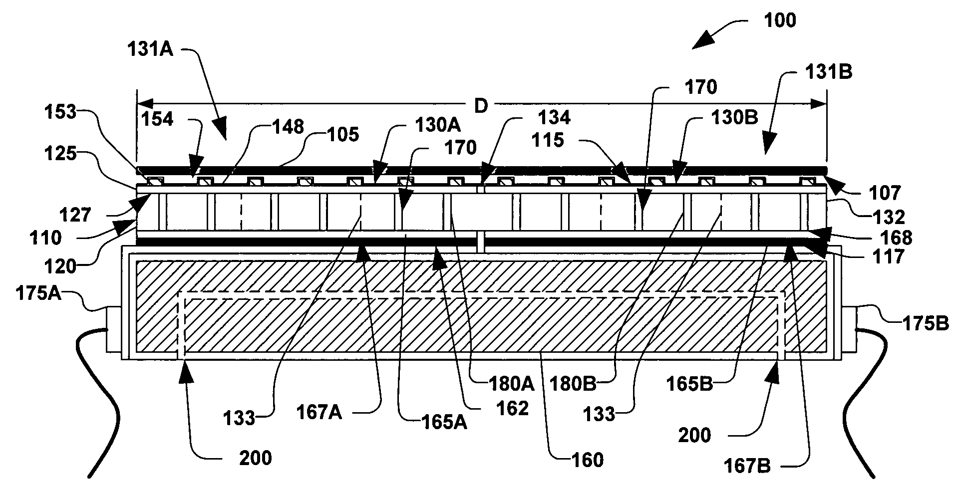
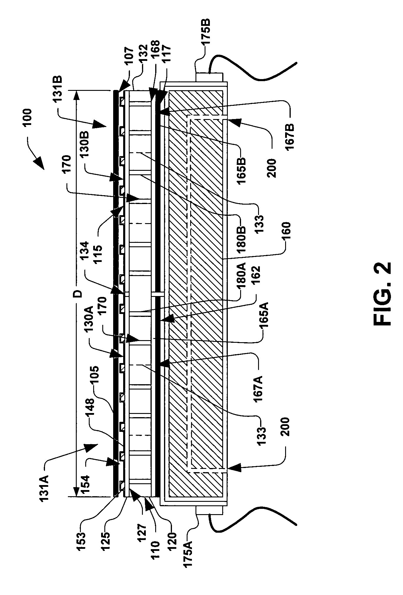
[0031] The present invention is directed towards a multi-polar electrostatic chuck (ESC) and an associated system and method that incorporate several inventive features thereof. In particular, the electrostatic chuck of the present invention increases an ability to uniformly heat or cool a wafer substrate. Accordingly, the present invention will now be described with reference to the drawings, wherein like reference numerals are used to refer to like elements throughout. It should be understood that the description of these aspects are merely illustrative and that they should not be taken in a limiting sense. In the following description, for purposes of explanation, numerous specific details are set forth in order to provide a thorough understanding of the present invention. It will be evident to one skilled in the art, however, that the present invention may be practiced without these specific details.

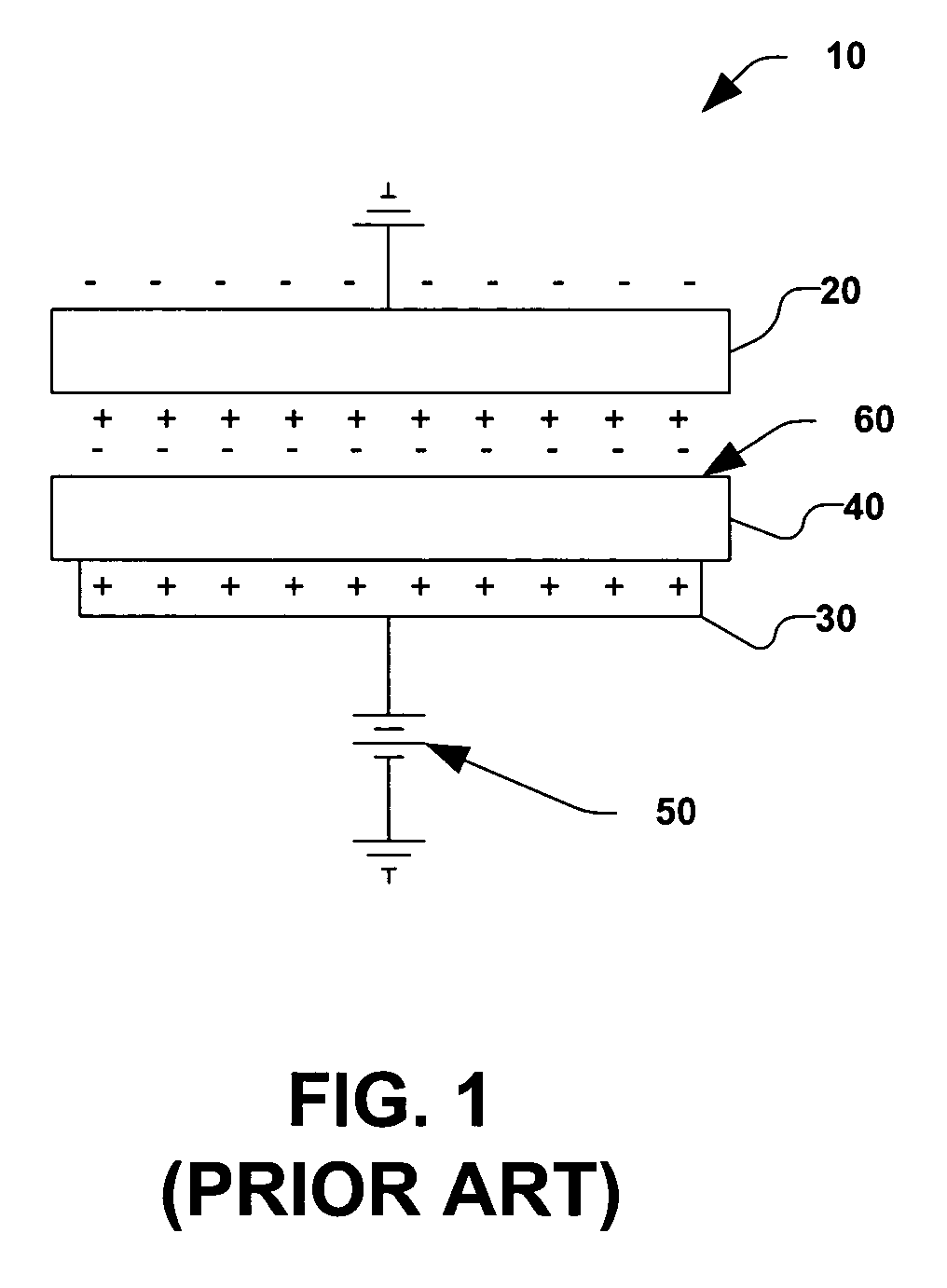
[0032] The present invention overcomes challenges of the prior art via a multi-...


PUM


Abstract

The present invention is directed to a method for clamping and processing a semiconductor substrate using a semiconductor processing apparatus. According to one aspect of the present invention, a multi-polar electrostatic chuck and associated method is disclosed which provides heating or cooling of a substrate by thermal contact conduction between the electrostatic chuck and the substrate. The multi-polar electrostatic chuck includes a semiconductor platform having a plurality of protrusions that define gaps therebetween, wherein a surface roughness of the plurality of protrusions is less than 100 Angstroms. The electrostatic chuck further includes a voltage control system operable to control a voltage applied to the electrostatic chuck to thus control a contact heat transfer coefficient of the electrostatic chuck, wherein the heat transfer coefficient of the electrostatic chuck is primarily a function of a contact pressure between the substrate and the plurality of protrusions.

Description

RELATED APPLICATIONS [0001] This application is related to, U.S. application Ser. No. 10 / 642,939, filed on Aug. 18, 2003, entitled, “MEMS Based Multi-polar Electrostatic Chuck”, and U.S. application Ser. No. 10 / 657,449, filed on Sep. 8, 2003, entitled, “Clamping and De-clamping Semiconductor Wafers on an Electrostatic Chuck Using Wafer Inertial Confinement by Applying a Single-Phase Square wave AC Clamping Voltage”, which are incorporated herein in their entirety, and U.S. application Ser. No. ______ , filed on , attorney docket No. 03-IMP-025, entitled, “Method of Making a MEMS Electrostatic Chuck”,FIELD OF THE INVENTION [0002] The present invention relates generally to semiconductor processing systems, and more specifically to an apparatus and method for clamping a substrate and transferring thermal energy associated therewith. BACKGROUND OF THE INVENTION [0003] Processing of silicon wafers is commonplace in the manufacture of modern microelectronics devices. Such processing, incl...

Claims


Application Information

Patent Timeline
Patent Type & Authority Applications(United States)
IPC IPC(8): H01L21/683
CPCY10S438/964H01L21/6831H01L21/683H01L21/687
Inventor KELLERMAN, PETER L.QIN, SHUALLEN, ERNIEBROWN, DOUGLAS A.
Owner AXCELIS TECHNOLOGIES
Why Eureka
Try Eureka