Method of cleaning a film-forming apparatus and film-forming apparatus

a film-forming apparatus and cleaning technology, applied in the direction of chemistry apparatus and processes, cleaning of hollow articles, coatings, etc., can solve the problems of cvd chamber generally made of quartz damaged by reactive gases, reducing productivity, and expensive plasma apparatus provided, so as to suppress the damage

Inactive Publication Date: 2005-04-21
LAIR LIQUIDE SA POUR LETUDE & LEXPLOITATION DES PROCEDES GEORGES CLAUDE
View PDF7 Cites 31 Cited by
  • Summary
  • Abstract
  • Description
  • Claims
  • Application Information

AI Technical Summary

Benefits of technology

[0010] Accordingly, an object of the present invention is to provide a method of cleaning a film-forming apparatus, which permits removing a silicon-based deposit while suppressing the damage done to a constituent member of the film-forming apparatus, and to provide a film-forming apparatus.

Problems solved by technology

Apparently, a long down time is required resulting in decreasing productivity.
However, for plasma cleaning, a costly plasma apparatus should be provided only for the cleaning purpose, although the plasma is not used in the CVD process.
With this cleaning method, the CVD chamber generally made of quartz is damaged by these reactive gases.
It should also be mentioned that especially in the cleaning of silicon nitride, life time of the CVD reaction chamber becomes remarkably shortened and high maintenance fee is required, because the cleaning rate of the cleaning object (silicon nitride) is almost the same as that of the quartz.
However, the ClF3 is a costly gas, increasing the cleaning cost.

Method used


Image

  • Method of cleaning a film-forming apparatus and film-forming apparatus
  • Method of cleaning a film-forming apparatus and film-forming apparatus
  • Method of cleaning a film-forming apparatus and film-forming apparatus

Examples


example 1

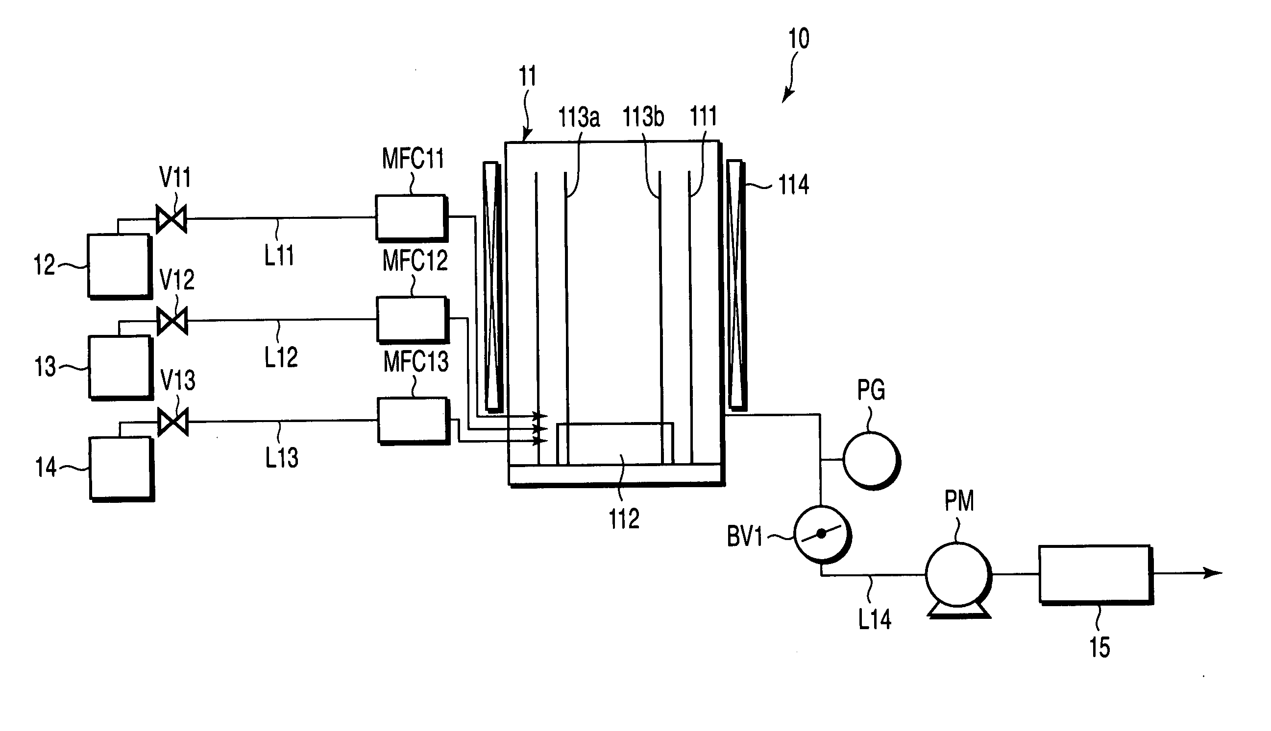
[0051] A sample having silicon nitride deposited thereon and a quartz sample were housed in a CVD reaction chamber. Then, fluorine gas and nitrogen monoxide gas were introduced into the CVD reaction chamber to carry out a cleaning operation under the conditions given below: [0052] Fluorine gas flow rate: 500 sccm [0053] Nitrogen monoxide gas flow rate: 200 sccm [0054] Nitrogen gas flow rate: 300 sccm [0055] Pressure inside the CVD reaction chamber: 50 Torr [0056] Cleaning temperature: 200° C.

[0057] As a result, the etching rate of the silicon nitride was found to be 3,500 Å / min and the etching rate of the quartz was found to be 220 Å / min. It follows that, in this Example, the etching selectivity of the silicon nitride film to quartz, i.e., a ratio. in the etching rate of the silicon nitride film to the quartz, was about 16, indicating that the silicon nitride film can be removed selectively.

example 2

[0058] A sample having silicon nitride deposited thereon and a quartz sample were housed in a CVD reaction chamber. Then, a cleaning operation was carried out by introducing fluorine gas and nitrogen monoxide gas into the CVD reaction chamber with the pressure inside the CVD reaction chamber set at 50 Torr and with the flow rates of the fluorine gas and the total gas set at 500 sccm and 1,000 sccm, respectively. In this case, the cleaning temperature was changed within a rage of 100° C. to 600° C. Also, the flow rate of the nitrogen monoxide gas was changed within a range of 100 sccm to 200 sccm. Note that nitrogen gas was introduced into the CVD reaction chamber such that the total gas flow rate was adjusted to 1,000 sccm. The results are shown in FIG. 4. In FIG. 4, curve a shown in relates to the case where the NO / F2 flow rate ratio was 0.2, and curve b relates to the case where the NO / F2 flow rate ratio was 0.4.

[0059] As apparent from FIG. 4, a maximum etching selectivity (silic...

example 3

[0060] A sample having silicon nitride deposited thereon and a quartz sample were housed in a CVD reaction chamber. Then, a cleaning operation was carried out by introducing fluorine gas and nitrogen monoxide gas into the CVD reaction chamber under the conditions that the pressure inside the CVD reaction chamber was set at 50 Torr, the cleaning temperature was set at 200° C., and the nitrogen monoxide gas flow rate and the total gas flow rate were set at 200 sccm and 1,000 sccm, respectively. In this case, the flow rate of the fluorine gas was changed within a range of 100 sccm to 500 sccm. Note that nitrogen gas was introduced into the CVD reaction chamber such that the total gas flow rate was adjusted to 1,000 sccm. The results are shown in FIG. 5. The shaded bar shown in FIG. 5 denotes the etching rate of silicon nitride, and the white bar denotes the etching rate of quartz. Further, curve a denotes the etching selectivity (silicon nitride / quartz).

[0061] As apparent from FIG. 5,...


PUM

PropertyMeasurementUnit
temperatureaaaaaaaaaa
pressureaaaaaaaaaa

Abstract

A method of cleaning a film-forming apparatus to remove at least a part of a silicon-based material deposited on a constituent member of the film-forming apparatus after used to form thin films includes introducing a first-gas including fluorine gas and a second gas including nitrogen monoxide gas into the film-forming apparatus, and heating the constituent member. The constituent member includes quartz or silicon carbide, and the silicon-based material includes silicon nitride.

Description

CROSS-REFERENCE TO RELATED APPLICATIONS [0001] This application is based upon and claims the benefit of priority from prior Japanese Patent Application No. 2003-209691, filed Aug. 29, 2003, the entire contents of which are incorporated herein by reference. BACKGROUND OF THE INVENTION [0002] 1. Field of the Invention [0003] The present invention relates to a method of cleaning a film-forming apparatus and a film-forming apparatus equipped with a cleaning system. [0004] 2. Description of the Related Art [0005] In manufacturing a semiconductor device, various (insulating) thin films such as a silicon dioxide film or a silicon nitride film are formed by using a film-forming apparatus comprising a chemical vapor deposition reaction chamber (CVD reaction chamber). In forming the thin film, the CVD reaction product is deposited not only on the surface of a target semiconductor wafer but also on the constituent member of the film-forming apparatus such as the wall of the CVD reaction chambe...

Claims


Application Information

Patent Timeline
Patent Type & Authority Applications(United States)
IPC IPC(8): B08B7/00C23C16/44
CPCB08B7/00B08B7/04C23C16/4405
Inventor SATO, YUUSUKETAMAOKI, NAOKISETA, SATOKOZILS, REGISSONOBE, JUNKIMURA, TAKAKOMOMODA, KAYO
Owner LAIR LIQUIDE SA POUR LETUDE & LEXPLOITATION DES PROCEDES GEORGES CLAUDE
Why Eureka
Try Eureka