ESD protection devices and methods of making same using standard manufacturing processes

Active Publication Date: 2005-04-21
ELECTRONICS POLYMERS NEWCO
View PDF15 Cites 73 Cited by
  • Summary
  • Abstract
  • Description
  • Claims
  • Application Information

AI Technical Summary

Benefits of technology

[0014] An advantage of the present invention is that protection devices can be manufactured in high volumes using well known printed circuit board (PCB) manufacturing techniques. With the present invention, a panel holding anywhere from several hundred up to many thousand protection devices can be achieved with a combination of mixing, coating, curing, lamination, photo etch, and electroding steps. As a result, application specific designs can be readily customized and changes made quickly with minimal effort and expense.
[0015] Another advantage is that added capacitance can be limited by controlling the size of the electrode, formulation fillers and overall thickness of the devices.
[0016] Another advantage of the present invention is the achievement of a low profile protection device compared to the known prior art. For example, a

Problems solved by technology

In general, such problems arise from the occurrence of electrical events that cause the transfer of charge from one material to another creating a surge in voltage due to voltage potential differences between the two materials.
While such techniques have been effectively used to shield the product from charge and to reduce the generation of charge caused by any movement of product within the container housing the device to be protected, they have not completely eliminated the risk of damage attributed to such disturbances.
Moreover, it is well known that more modem devices operating in the higher frequencies (GHz and above) using submicron line widths are more susceptible to damage which can not be overcome using such methods.
Such prior art protection component

Method used


Image

  • ESD protection devices and methods of making same using standard manufacturing processes
  • ESD protection devices and methods of making same using standard manufacturing processes
  • ESD protection devices and methods of making same using standard manufacturing processes

Examples


Embodiment Construction

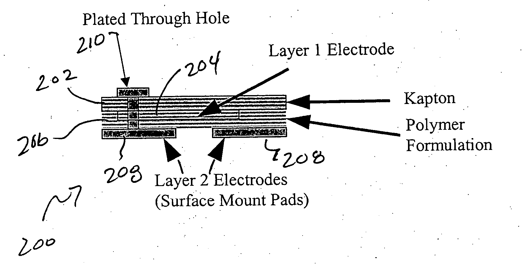
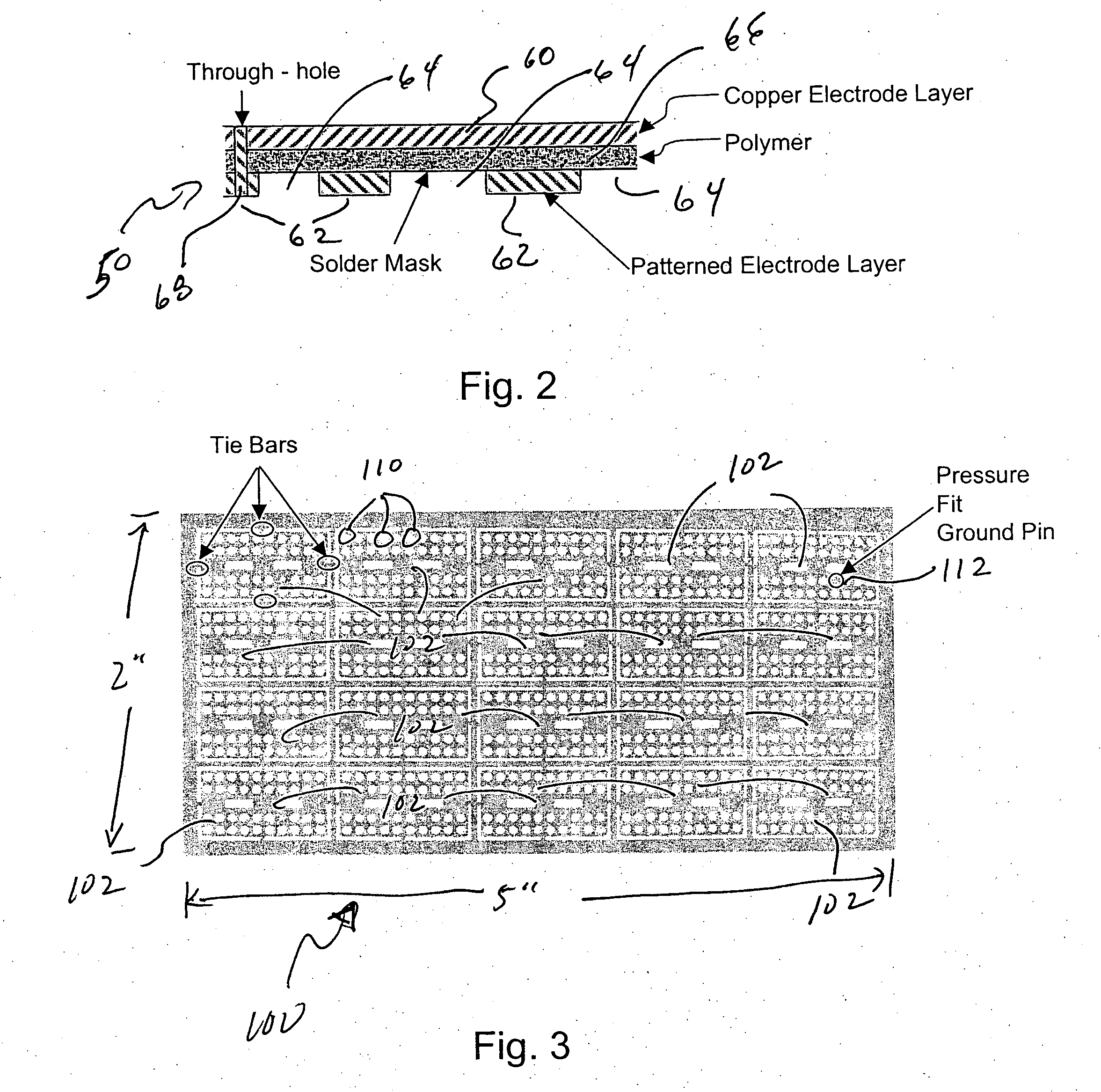
[0029] The present invention provides a process of making a substrate-less protection device using standard printed circuit board (PCB) manufacturing techniques thereby allowing the manufacture of large number of devices relatively inexpensively. With the present invention, multiple ESD protection devices can be manufactured in panels that can be custom formed for an unlimited number of applications. It is believed that the process of the present invention has implications toward the manufacture of an all PCB protection system such as flex circuit with total ESD protection and / or as a layer in a PCB with protection provided for sensitive integrated circuits.

Manufacturing a Protection Device in Panels Gives Maximum Yield in High Quantities

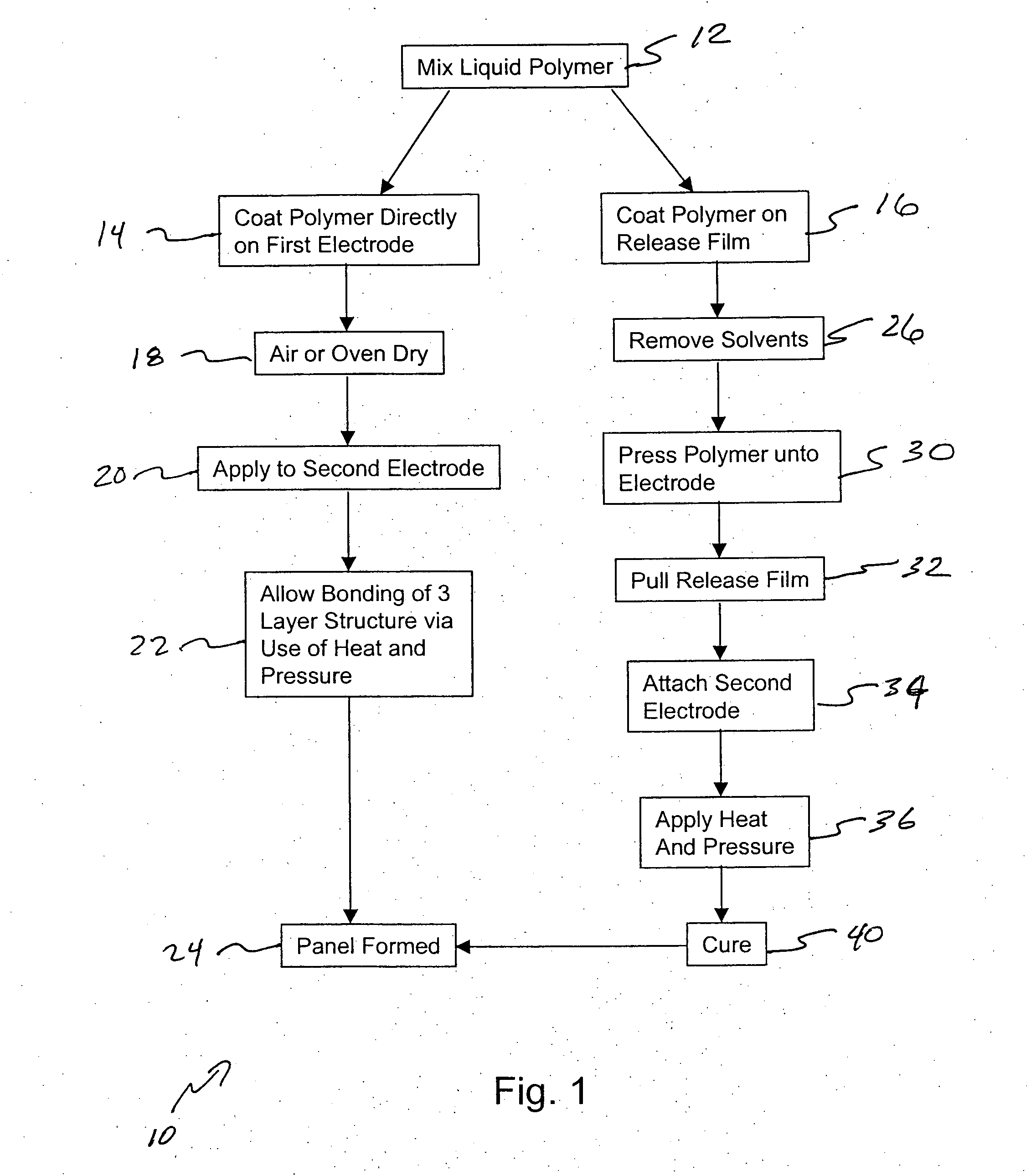
[0030] In general, the process of building a protection device according to the invention involves the use of a polymer-based formulation (or polymeric solution) that is coated directly on the electrodes forming the terminals of the protection de...


PUM

PropertyMeasurementUnit
Electrical conductoraaaaaaaaaa

Abstract

Devices capable of protecting electronic components during the occurrence of a disturbance event using printed circuit board manufacturing techniques. A three (3) layer structure is formed comprising a polymer-based formulation sandwiched between two electrode layers. The devices can be manufactured in panel form providing high quantities of devices which can be removed from the panel and applied directly to the component to be protected. Desired patterns can be formed on either one of the electrode layers by photo-etch techniques thereby providing a process that can be tailored to a large number of applications.

Description

TECHNICAL FIELD [0001] The present invention relates to electronic circuit protection devices and methods of making same. More particularly, the invention relates to the use of standard printed circuit board manufacturing processes for mass production of low profile polymer-based protection devices. Still more particularly, the invention relates to the manufacture of substrate-less protection devices that can be custom formed for use in a wide array of electronic circuit protection applications, such as electrostatic discharge and surge suppression, with possible implications toward the manufacture of a complete PCB protection system. Even still more particularly, the method of making such devices takes advantage of the vast know-how used in making printed circuit wiring boards and allows devices to be made in panels with features such as plated through-holes and multiple layers. BACKGROUND OF THE INVENTION [0002] The problems of static electricity and Electrostatic Discharge (ESD) ...

Claims


Application Information

Patent Timeline
IPC IPC(8): H01C7/00H01C17/065H01R13/648H05K1/02H05K1/03H05K1/16
CPCH01C7/005H01C17/06586H01R13/6485H05K1/0259H05K1/0373H05K1/167Y10T29/49222H05K2201/0738Y10T29/49195Y10T29/49146Y10T29/49156Y10T29/49155Y10T29/49107H05K3/0052
Inventor SHRIER, KAREN P.
Owner ELECTRONICS POLYMERS NEWCO
Why Eureka
Try Eureka