

Heterogeneous activation layers formed by ionic and electroless reactions used for IC interconnect capping layers
a technology of ic interconnection and activation layer, which is applied in the direction of liquid/solution decomposition chemical coating, coating, metallic material coating process, etc., can solve the problems of reducing the reliability of the overall circuit, increasing the resistance, and easy formation of copper oxide by copper
- Summary
- Abstract
- Description
- Claims
- Application Information
AI Technical Summary
Problems solved by technology
Method used
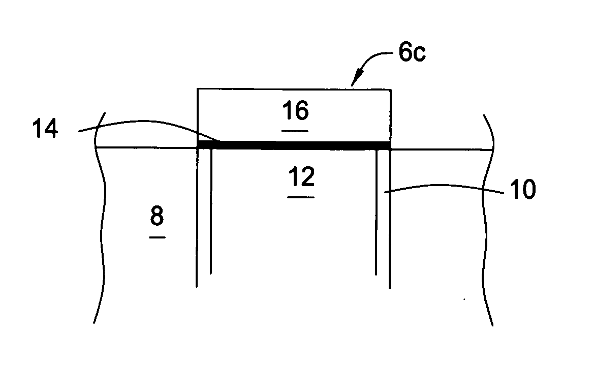
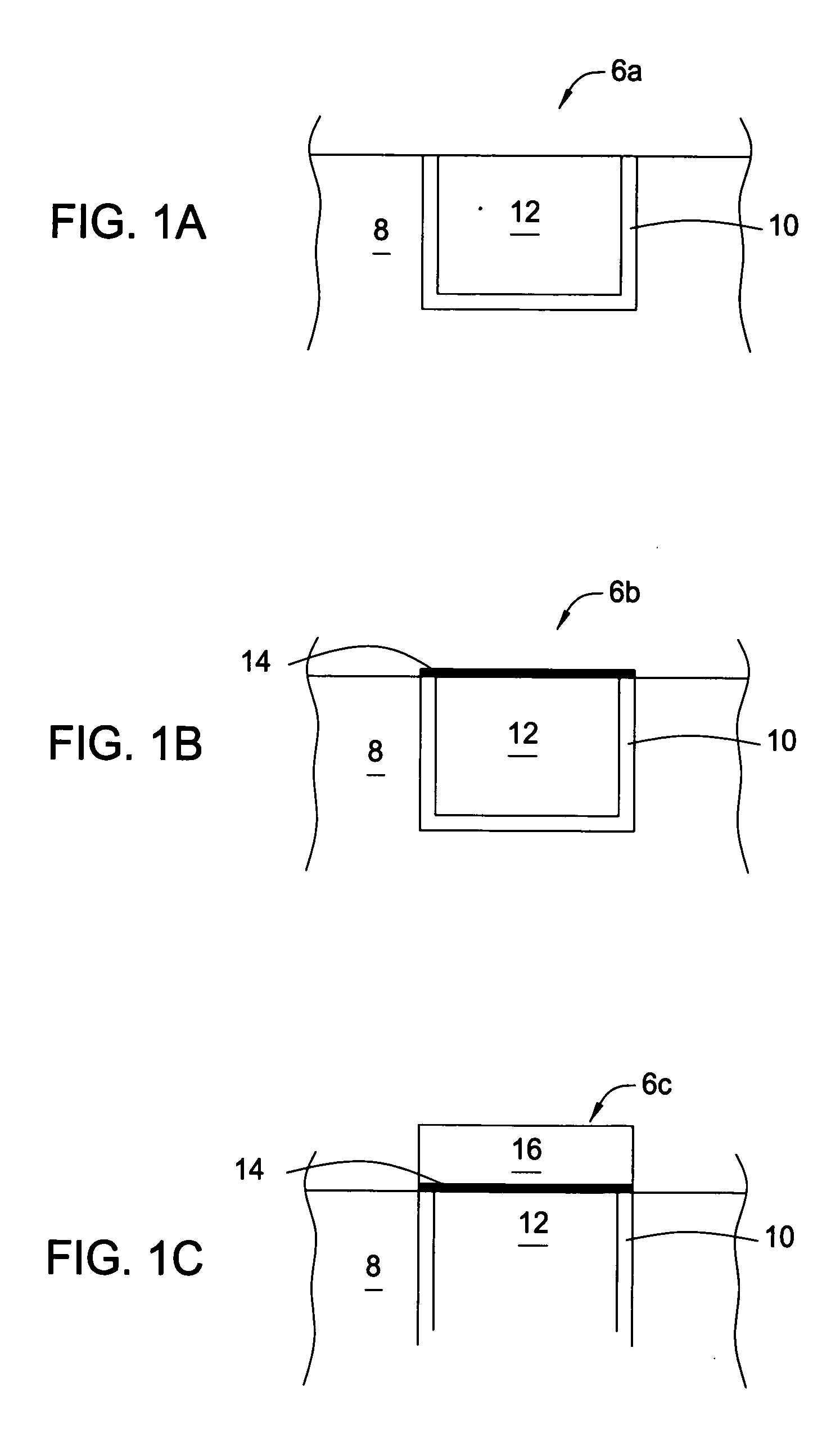
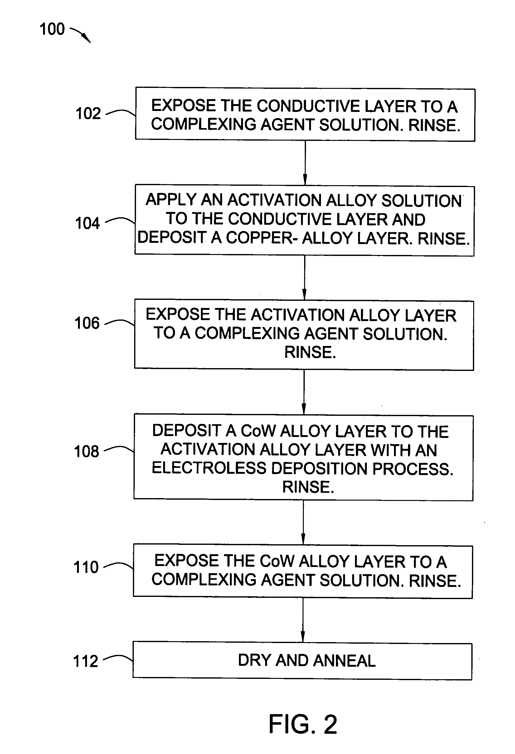
Image

Examples
example 1
[0086] An activation-alloy solution includes the following concentration: CuSO4.5H2O from about 15 g to about 30 g; PdSO4.7H2O from about 15 g to about 100 g; citric acid from about 50 g to about 80 g; tartaric acid from about 50 g to about 80 g; DMAB from about 5 g to about 20 g; RE-610 from about 50 ppm to about 500 ppm; NH4OH to a pH on the range from about 7 to about 12, preferably from about 9 to about 12; and deionized water to form about 1 L.
example 2
[0087] An activation-alloy solution includes the following concentration: CuSO4.5H2O from about 15 g to about 30 g; PdSO4.7H2O from about 15 g to about 100 g; glyoxylic acid from about 50 g to about 80 g; tartaric acid from about 50 g to about 80 g; RE-610 from about 50 ppm to about 500 ppm; TMAH to a pH on the range from about 7 to about 12, preferably from about 9 to about 12; and deionized water to form about 1 L.
example 3
[0088] An activation-alloy solution includes the following concentration: CuSO4.5H2O from about 15 g to about 30 g; PdSO4.7H2O from about 15 g to about 100 g; citric acid from about 50 g to about 80 g; H3PO2 from about 5 g to about 40 g; RE-610 from about 50 ppm to about 500 ppm; NH4OH to a pH on the range from about 7 to about 12, preferably from about 9 to about 12; and deionized water to form about 1 L.
PUM
| Property | Measurement | Unit |
|---|---|---|
| temperature | aaaaa | aaaaa |
| exposure time | aaaaa | aaaaa |
| exposure time | aaaaa | aaaaa |
Abstract
Description
Claims
Application Information