Multi-chip module and method for testing

a multi-chip module and multi-chip technology, applied in the direction of solid-state devices, semiconductor/solid-state device details, instruments, etc., can solve the problems of defective memory cells identified as defective, laser fuses can only be programmed during and no longer, and memory cells that cannot be repaired can no longer be programmed. , to achieve the effect of increasing the yield

Inactive Publication Date: 2005-04-21
INFINEON TECH AG
View PDF11 Cites 14 Cited by
  • Summary
  • Abstract
  • Description
  • Claims
  • Application Information

AI Technical Summary

Benefits of technology

[0013] An additional advantage results from the fact that defective memory cells can be identified and repaired even during normal operation. For this purpose a special test program which, for example after the activation of the integrated circuit, tests the integrated semiconductor memory and automatically repairs defective memory cells that are possibly present may be stored in the integrated circuit, for example in a microcontroller therein. In this example case, a repair is to be understood as the permanent storage of the addresses of the defective memory cells in such a way that in the event of accesses to the defective memory cells a divers

Problems solved by technology

On account of the physical conditions during the fabrication of integrated semiconductor chips in mass production methods it is practically inevitable that some of the multiplicity of memory cells in integrated semiconductor memories will be defective actually during or after production.
Howeve

Method used


Image

  • Multi-chip module and method for testing
  • Multi-chip module and method for testing
  • Multi-chip module and method for testing

Examples


Embodiment Construction

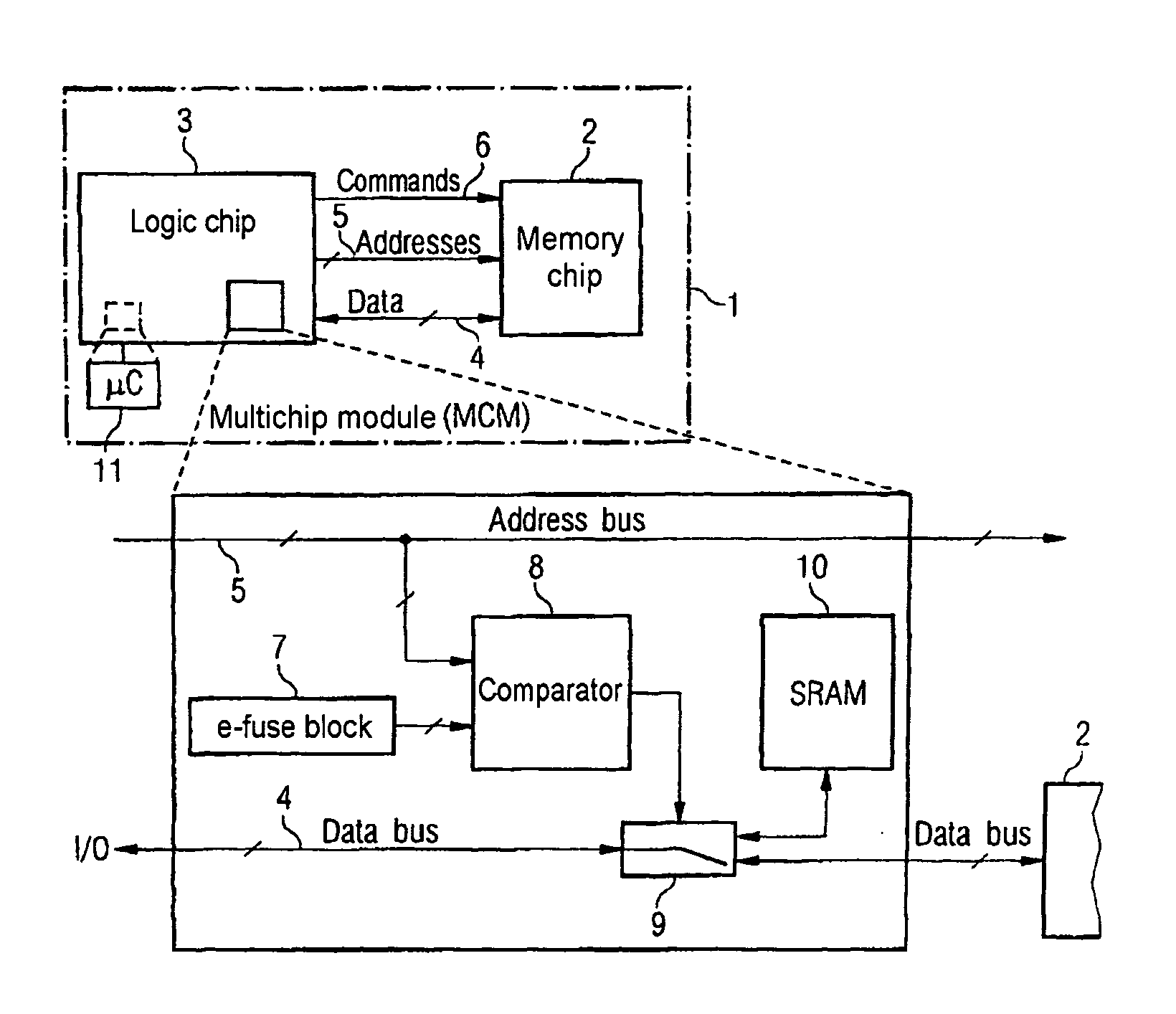
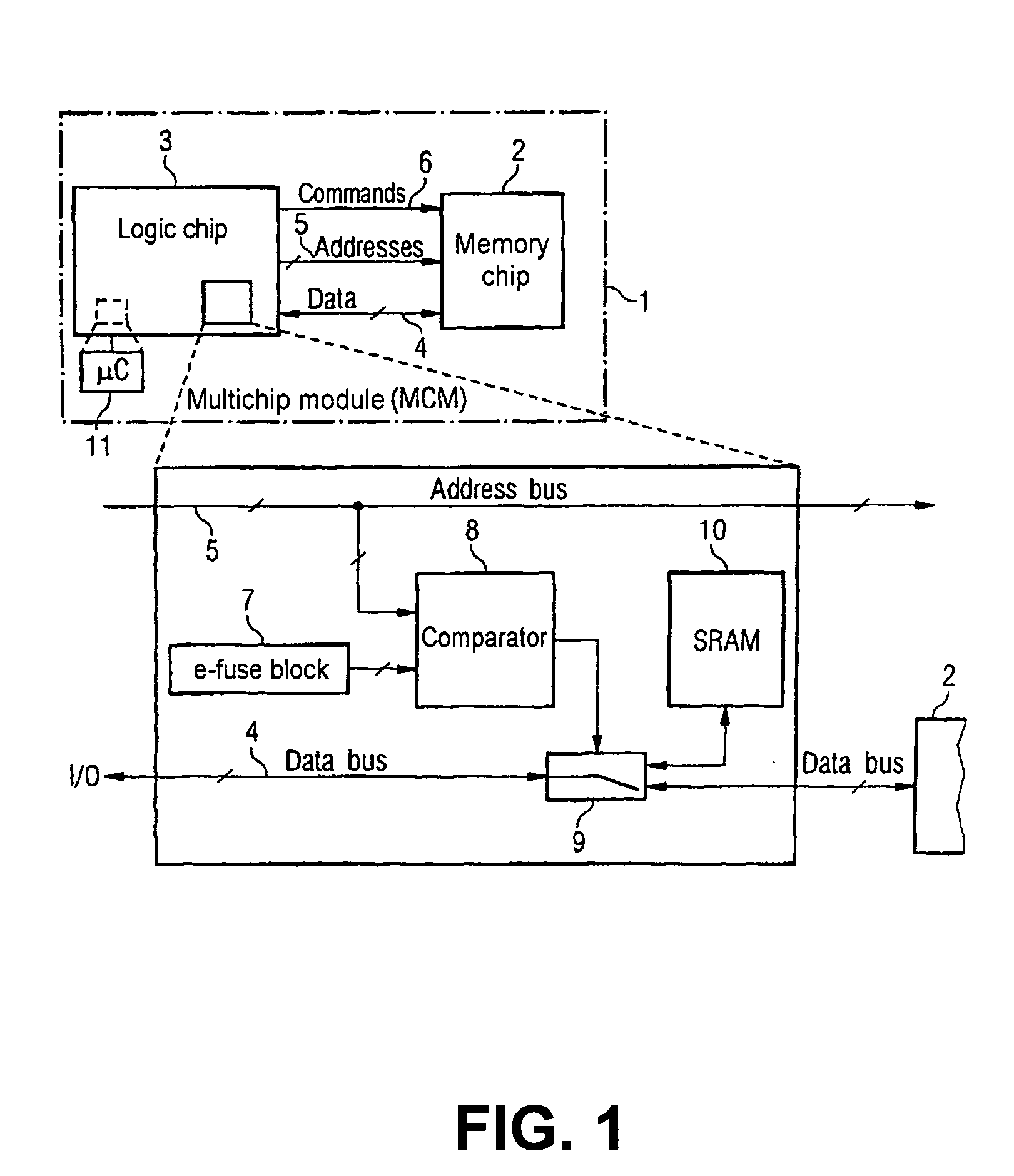
[0033]FIG. 1 shows a multi-chip module 1 according to one aspect of the present invention. The multi-chip module 1 comprises by way of example only one integrated semiconductor memory 2 and an integrated circuit 3 embodied as a logic chip. The integrated semiconductor memory 2 and the integrated circuit 3 are separate integrated circuits. The latter are applied on a common carrier, for example a printed circuit board, in order to form the multi-chip module 1. The integrated circuit 3 and the integrated semiconductor memory 2 are connected to one another via a bidirectional data bus 4 and an address bus 5 from the integrated circuit 3 to the semiconductor memory 2 and a command line 6 which likewise connects the integrated circuit 3 to the integrated semiconductor memory 2.

[0034] The integrated circuit 3 comprises a block 7 having a multiplicity of electrically programmable links embodied as so-called e-fuses. The latter serve to store addresses of memory cells in the integrated sem...


PUM


Abstract

A multi-chip module having an integrated semiconductor mass memory and a logic chip is disclosed. In accordance with one aspect of the invention, the integrated logic chip includes electrically programmable links or other non-volatile memory for permanently storing memory cells of the memory chip identified as defective. In the event of accesses to the memory chip the address present is compared with the stored addresses of the defective cells by a comparator and, if appropriate, a changeover is made from the memory chip to a volatile memory provided for this purpose in the logic chip, in which redundant memory cells are formed. The result is a significantly increased yield and a reduced test complexity, particularly in mass production.

Description

REFERENCE TO RELATED APPLICATIONS [0001] This application claims the benefit of the priority date of German application DE 103 39 054.5, filed on Aug. 25, 2003, the contents of which are herein incorporated by reference in their entirety. FIELD OF THE INVENTION [0002] The present invention relates to a multi-chip module and to a method for testing a multi-chip module. BACKGROUND OF THE INVENTION [0003] A multi-chip module normally comprises a plurality of integrated semiconductor circuits, so-called chips. By way of example, it is customary for such a multi-chip module to have one or a plurality of integrated semiconductor memories and also a logic chip. The integrated semiconductor memory or memories is or are in this case usually designed as volatile memories in the form of Dynamic Random Access Memories, DRAM. For driving the memory chips the logic chip is normally coupled thereto via a data bus, an address bus and one or more command lines. [0004] On account of the physical cond...

Claims


Application Information

Patent Timeline
IPC IPC(8): G01R31/3185G11C29/00H01L23/02
CPCG01R31/318505G11C29/846G11C29/78G01R31/318513
Inventor FRANKOWSKY, GERDOSSIMITZ, PETER
Owner INFINEON TECH AG
Why Eureka
Try Eureka