Sidewall formation for high density polymer memory element array

a memory element array and polymer technology, applied in the field of semiconductor structure fabrication, can solve the problems of limited lithographic resolution, reduced lithographic resolution, and reduced lithographic resolution, so as to facilitate the deposit of conductivity facilitating compound and enhance chemical vapor deposition

Active Publication Date: 2005-05-05
CYPRESS SEMICON CORP
View PDF8 Cites 12 Cited by
  • Summary
  • Abstract
  • Description
  • Claims
  • Application Information

AI Technical Summary

Benefits of technology

[0015] Furthermore, according to another aspect of the present invention, the passive layer is deposited on to the conductive layer via a plasma enhanced chemical vapor deposition (PECVD) employing a metal organic precursor. The precursor facilitates depositing the conductivity facilitating compound in the absence of the toxic hydrogen sulphide and at a relatively low temperature and pressure (e.g. between about 473 to 573 K and 0.2 Pa., respectively.)

Problems solved by technology

Volatile memory cells usually lose their information if they lose power and typically require periodic refresh cycles to maintain their information.
Nonetheless, defining smaller as well as denser features, is limited to the lithographic resolution processes employed in creating these features.
As such, the lithographic resolution affects, and the minimum feature size as well as the creation of the various features of the memory cells, is thus limited by the lithographic resolution.

Method used


Image

  • Sidewall formation for high density polymer memory element array
  • Sidewall formation for high density polymer memory element array
  • Sidewall formation for high density polymer memory element array

Examples


Embodiment Construction

[0040] The present invention is now described with reference to the drawings, wherein like reference numerals are used to refer to like elements throughout. In the following description, for purposes of explanation, numerous specific details are set forth in order to provide a thorough understanding of the present invention. It may be evident, however, that the present invention may be practiced without these specific details.

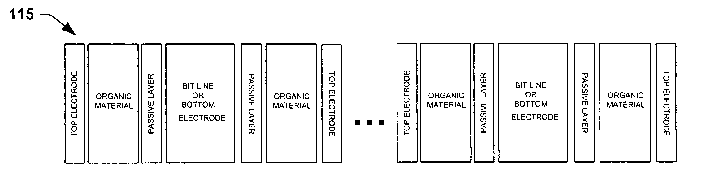
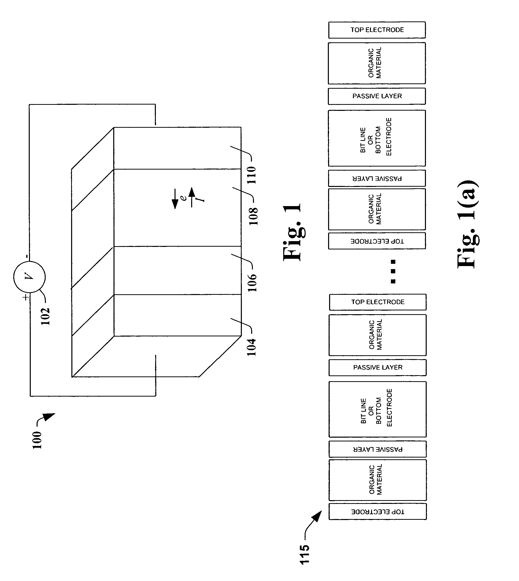
[0041] The present invention provides for a system and methodology for increasing number of organic memory cells associated with a lithographic feature, wherein memory elements are formed on sidewalls of the lithographic feature.

[0042] Such a multi-cell and multi-layer organic memory component can be formed with two or more electrodes having a selectively conductive media between the electrodes forming individual cells, while employing a partitioning component to enable lateral stacking of additional memory cells adjacent or in association with previously for...


PUM


Abstract

Systems and methodologies are disclosed for increasing the number of memory cells associated with a lithographic feature. The systems comprise memory elements that are formed on the sidewalls of the lithographic feature by employing various depositing and etching processes. The side wall memory cells can have a bit line of the wafer as the first electrode and operate with a second formed electrode to activate a portion of an organic matter that is formed there between.

Description

FIELD OF THE INVENTION [0001] The present invention relates generally to semiconductor structure fabrication and, in particular to a system and methodology for forming memory elements in a semiconductor chip. BACKGROUND OF THE INVENTION [0002] The proliferation and increased usage of portable computer and electronic devices has greatly increased demand for memory cells. Digital cameras, digital audio players, personal digital assistants, and the like generally seek to employ large capacity memory cells (e.g., flash memory, smart media, compact flash, or the like). Memory cells can generally be subdivided into volatile and non-volatile types. Volatile memory cells usually lose their information if they lose power and typically require periodic refresh cycles to maintain their information. Volatile memory cells include, for example, random access memory (RAM), DRAM, SRAM and the like. Non-volatile memory cells maintain their information whether or not power is maintained to the device...

Claims


Application Information

Patent Timeline
Patent Type & Authority Applications(United States)
IPC IPC(8): G11C11/56G11C13/02H01L27/115H01L27/28H01L29/68H01L45/00H01L51/00
CPCB82Y10/00G11C11/5664H01L51/0595G11C13/0016H01L27/285G11C13/0014H10K19/202H10K10/701H01L21/3213
Inventor LYONS, CHRISTOPHER F.CHANG, MARK S.LOPATIN, SERGEY D.SUBRAMANIAN, RAMKUMARCHEUNG, PATRICK K.NGO, MINH V.OGLESBY, JANE V.
Owner CYPRESS SEMICON CORP
Why Eureka
Try Eureka