
Semiconductor light emitting device and method of manufacturing the same

Inactive Publication Date: 2005-05-12
ROHM CO LTD
View PDF15 Cites 6 Cited by
  • Summary
  • Abstract
  • Description
  • Claims
  • Application Information

AI Technical Summary

Benefits of technology

[0015] Moreover, it is another object of the invention to provide a semiconductor light emitting device which reduces a stress to be applied to a mesa section in both film formation and use and has a high reliability.
[0049] Furthermore, it is desirable that the temperature of the precursor solution should be raised and a precrosslinking step of starting a crosslinking reaction should be included, and the precursor solution starting a crosslinking reaction at the precrosslinking step should be caused to come in contact with the substrate prior to the contact step. According to such a method, the precrosslinking is carried out in advance and the precursor solution is then caused to come in contact with the surface of the substrate. Consequently, the crosslinking can efficiently progress and a thin film having a low dielectric constant and a high reliability can be formed at a high speed.

Problems solved by technology

Consequently, there is a problem in that an increase in the modulating speed of the laser is impeded.
However, the polyimide has a great difference in a coefficient of thermal expansion from the mesa section.
Consequently, peeling is generated on an interface, resulting in a deterioration in a reliability in some cases.

Method used


Image

  • Semiconductor light emitting device and method of manufacturing the same
  • Semiconductor light emitting device and method of manufacturing the same
  • Semiconductor light emitting device and method of manufacturing the same

Examples


first embodiment

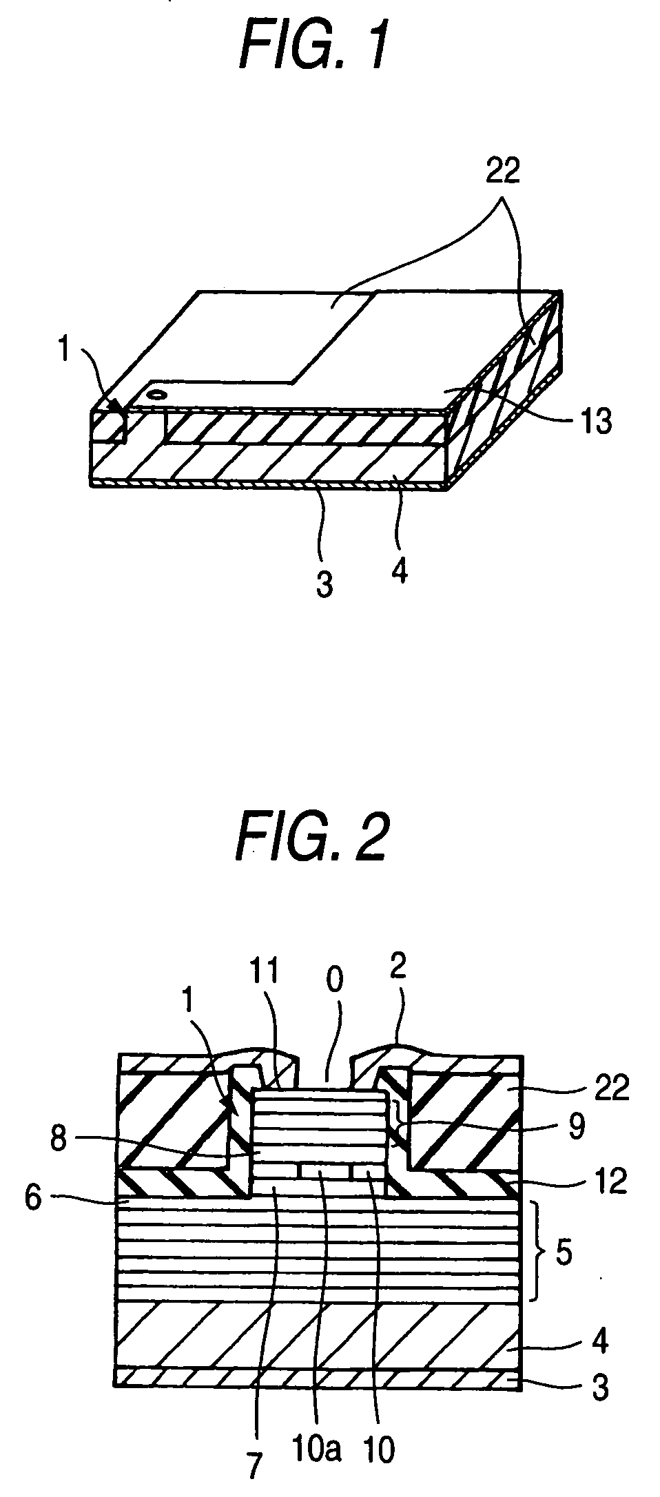
[0064] As a first embodiment of the invention, description will be given to a surface emission type semiconductor laser using, as an insulating layer, a thin film having a low dielectric constant formed by a method according to the invention.

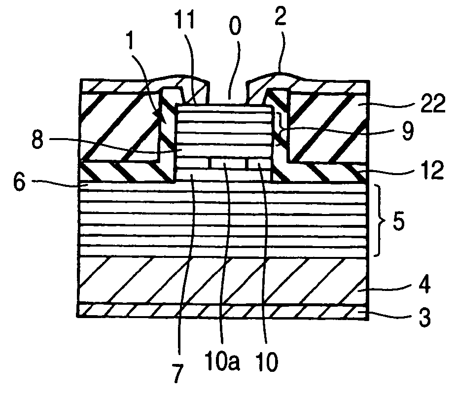
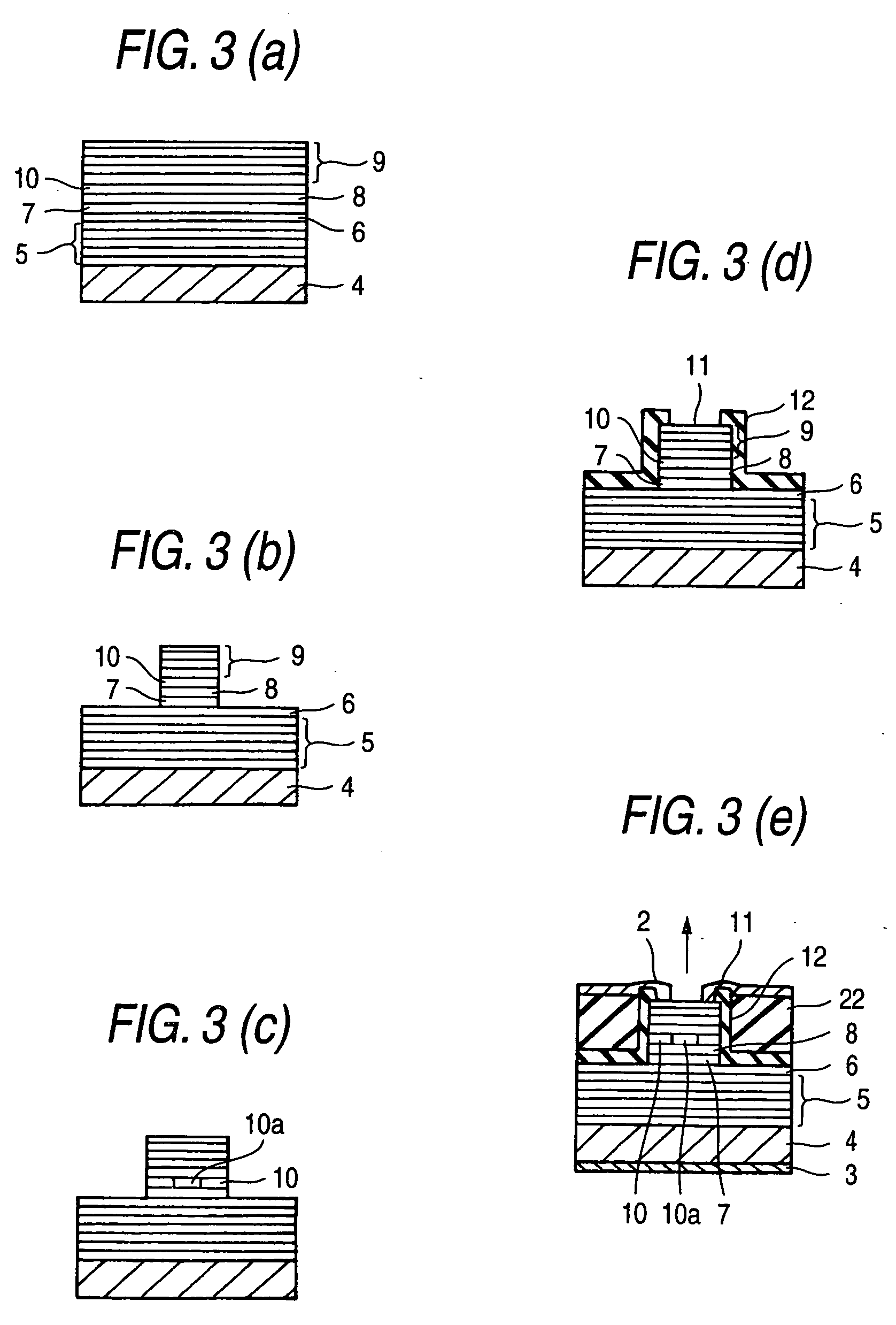
[0065] The surface emission type semiconductor laser according to the first embodiment of the invention is characterized in that an insulating film provided under a pad 13 is constituted by a thin film having a low dielectric constant as shown in FIG. 1 to be a perspective view, FIG. 2 to be an enlarged sectional view showing a main part, FIG. 3 to be a view showing a manufacturing process, and FIGS. 4 and 5 to be a typical view showing the structure of an insulating film according to the embodiment and a view showing a manufacturing process.

[0066] The structure of a mesa section to be a light emitting section is the same as that of the semiconductor laser according to the conventional example shown in FIGS. 11 and 12 and detailed description ...

second embodiment

[0103] While the surface emission type semiconductor laser having the mesa structure has been described in the first embodiment, this is not restricted but the invention can also be applied to a surface emission type semiconductor laser having a trench structure shown in FIG. 7.

[0104] This structure is characterized in that the mesa section in the first embodiment is surrounded by a trench and the trench is filled with the thin film 22 having a low dielectric constant. 2 denotes an electrode.

[0105] With such a structure, it is also possible to provide a surface emission type semiconductor laser in which the mechanical strength of the mesa section can be increased and a pad capacity can be reduced.

[0106] For a dip coating method, a method of dropping a precursor solution onto a substrate is also effective in addition to the method described above.

third embodiment

[0107] While the thin mesoporous silica film is formed by carrying out the spin coating method over the precursor solution in the first embodiment, the spin coating method is not restricted but a dipping method may be carried out as shown in FIGS. 8(a) and 8(b).

[0108] In the same manner as in the embodiment, as shown in FIG. 8(a), mixing is carried out to prepare a precursor solution and a substrate 4 having the mesa section formed thereon is dipped in the solution as shown in FIG. 8(b). The substrate 4 subjected to the application is held overnight at 90° C. to polymerize the silica derivative by hydrolysis (a polycondensation reaction) (a precrosslinking step), thereby forming a thin mesoporous silica film in which the periodic autoagglutinin of a surface active agent is set to be a template.

[0109] In the same manner as in the first embodiment, finally, the substrate 4 is held for two nights at 90° C. to polymerize the silica derivative by a hydrolysis and polycondensation react...


PUM


Abstract

In a semiconductor light emitting device including a mesa section having at least a sandwich structure of an n-type clad layer, an active layer and a p-type clad layer which are constituted by compound semiconductor layers formed on a substrate, and an inorganic insulating film 22 formed to cover the mesa section excluding a contact region, the inorganic insulating film is constituted by an inorganic insulating film having a vacancy rate of 50% or more.

Description

BACKGROUND OF THE INVENTION [0001] 1. Field of the Invention [0002] The present invention relates to a semiconductor light emitting device and a method of manufacturing the semiconductor light emitting device, and more particularly to a reduction in the parasitic capacitance of an electrode pad section. [0003] 2. Description of the Related Art [0004] A semiconductor light emitting device using a compound semiconductor, particularly, a compound semiconductor laser has widely been used in an optical apparatus. FIG. 11 is a perspective view typically showing an example of the compound semiconductor laser and FIG. 12 is a sectional view showing a main part. As shown in the drawings, a compound semiconductor laser 1 is constituted by a first electrode 3, a second electrode 2 and a plurality of compound semiconductor layers provided between the first electrode 3 and the second electrode 2. [0005] The compound semiconductor layer is constituted by a semiconductor substrate 4 (for example, ...

Claims


Application Information

Patent Timeline
IPC IPC(8): H01S5/227H01L27/15H01S5/042H01S5/183H01S5/22
CPCH01L33/44H01S5/0425H01S2301/176H01S5/18311H01S5/06226H01S5/04252H01S5/04254
Inventor SAI, HIRONOBUOKU, YOSHIAKI
Owner ROHM CO LTD
Learn More