Low rise/fall skewed input buffer compensating process variation

a buffer and process variation technology, applied in logic circuits, oscillation generators, reliability increasing modifications, etc., can solve the problems of skew between rise and fall times, high sensitive current flow through nmos and pmos transistors, etc., and achieve the effect of minimizing skew

Inactive Publication Date: 2005-05-19
POLARIS INNOVATIONS
View PDF2 Cites 7 Cited by
  • Summary
  • Abstract
  • Description
  • Claims
  • Application Information

AI Technical Summary

Benefits of technology

[0010] The present invention generally provides an improved buffer circuit that minimizes ske...

Problems solved by technology

However, current flow through NMOS and PMOS transistors is highly sensitive to process variations (e.g., variations in supply voltages or operating t...

Method used


Image

  • Low rise/fall skewed input buffer compensating process variation
  • Low rise/fall skewed input buffer compensating process variation
  • Low rise/fall skewed input buffer compensating process variation

Examples


Embodiment Construction

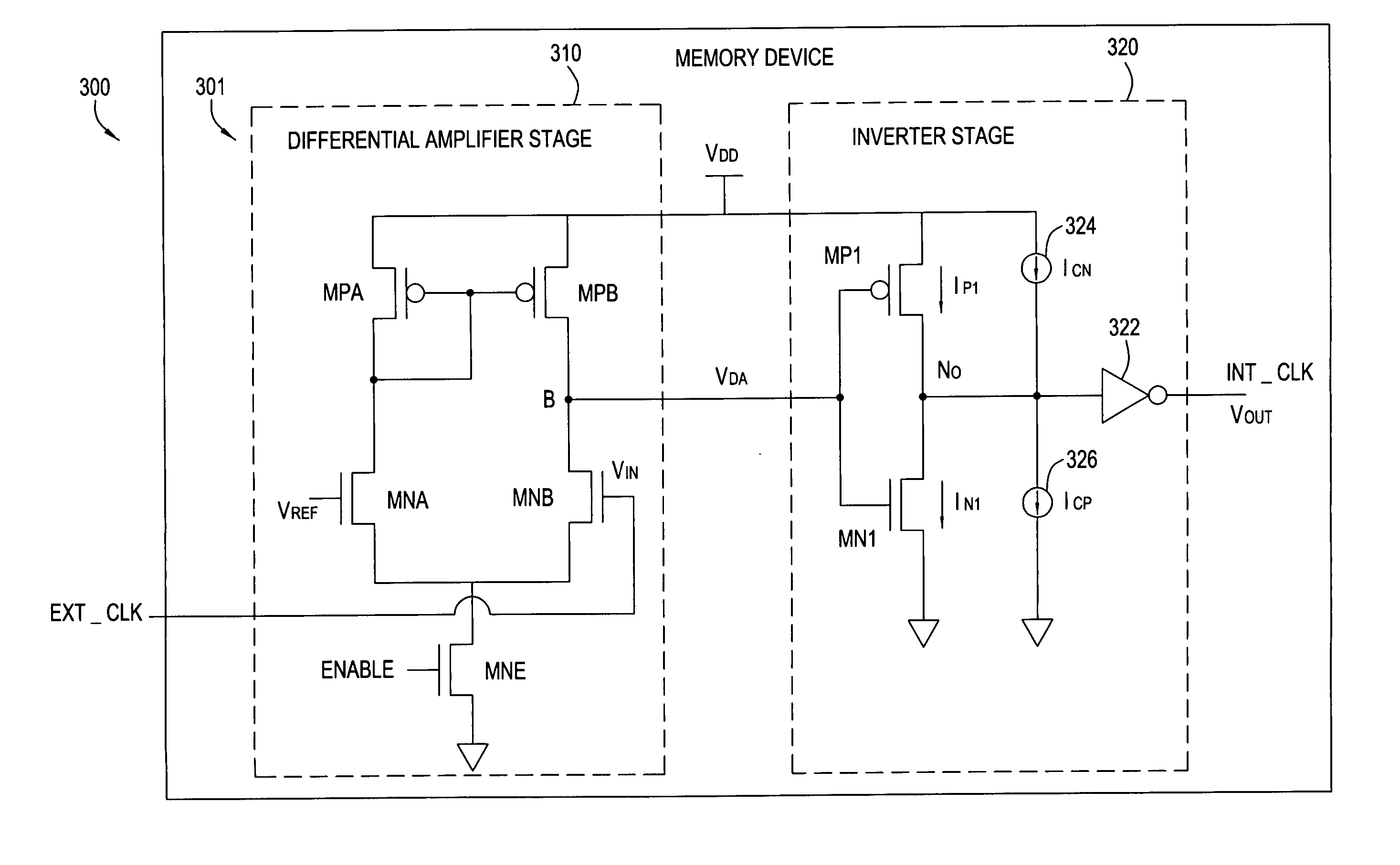
[0022] The present invention generally provides an improved buffer circuit that minimizes skew between rising and falling edges of output data as process conditions vary. As previously described, variations in process conditions may result in stronger or weaker relative current drive between NMOS and PMOS transistors. For some embodiments, one or more process-dependent current sources may be utilized to compensate for process variations by supplementing the current drive of transistors used to precharge (PMOS) or discharge (NMOS) an output node of a secondary (e.g., inverter) stage of the buffer circuit. As a result, rise and fall times of data output by the secondary stage may be more closely matched, thus minimizing skew.

[0023] For example, as NMOS transistor current drive gets stronger, current from a compensating current source may supplement (relatively weaker) PMOS transistor current drive. As NMOS current drive gets weaker, current flow through the one or more compensating t...


PUM


Abstract

Buffer circuits and techniques that reduce skew between rising and falling times of output data as process conditions vary are provided. One or more process-dependent current sources may be utilized to compensate for process variations by supplementing the current drive of transistors used to precharge (PMOS) or discharge (NMOS) an output node of a secondary (e.g., inverter) stage of the buffer circuit.

Description

BACKGROUND OF THE INVENTION [0001] 1. Field of the Invention [0002] The present invention generally relates to integrated circuit devices and, more particularly to buffer circuits utilized in integrated circuit devices. [0003] 2. Description of the Related Art [0004] Integrated circuit devices (ICs) utilize input buffers for a variety of purposes, such as receiving input signals supplied from an external device and supplying a “buffered version” of the input signals to some other portion of the IC for processing. As illustrated in FIG. 1, a conventional input buffer 100 typically utilizes two stages: a differential amplifier stage 110 and a simple inverter stage 120. [0005] The differential amplifier stage 110 typically receives an input signal (VIN) applied to one input and a reference voltage (VREF) applied to another input. As illustrated, the differential amplifier stage 110 includes an arrangement of PMOS transistors (MPA and MPB) and NMOS transistors (MNA, MNB, and MNE). The d...

Claims


Application Information

Patent Timeline
IPC IPC(8): H03K19/003
CPCH03K19/00323H03K19/00384
Inventor HAN, JONGHEE
Owner POLARIS INNOVATIONS
Why Eureka
Try Eureka