

Stressed semiconductor device structures having granular semiconductor material
a semiconductor and granular technology, applied in the direction of semiconductor devices, electrical equipment, transistors, etc., can solve the problems of difficult control of stress properties, and achieve the effects of improving device performance, preventing compressive stress, and improving mobility
- Summary
- Abstract
- Description
- Claims
- Application Information
AI Technical Summary
Benefits of technology
Problems solved by technology
Method used
Image

Examples
Embodiment Construction
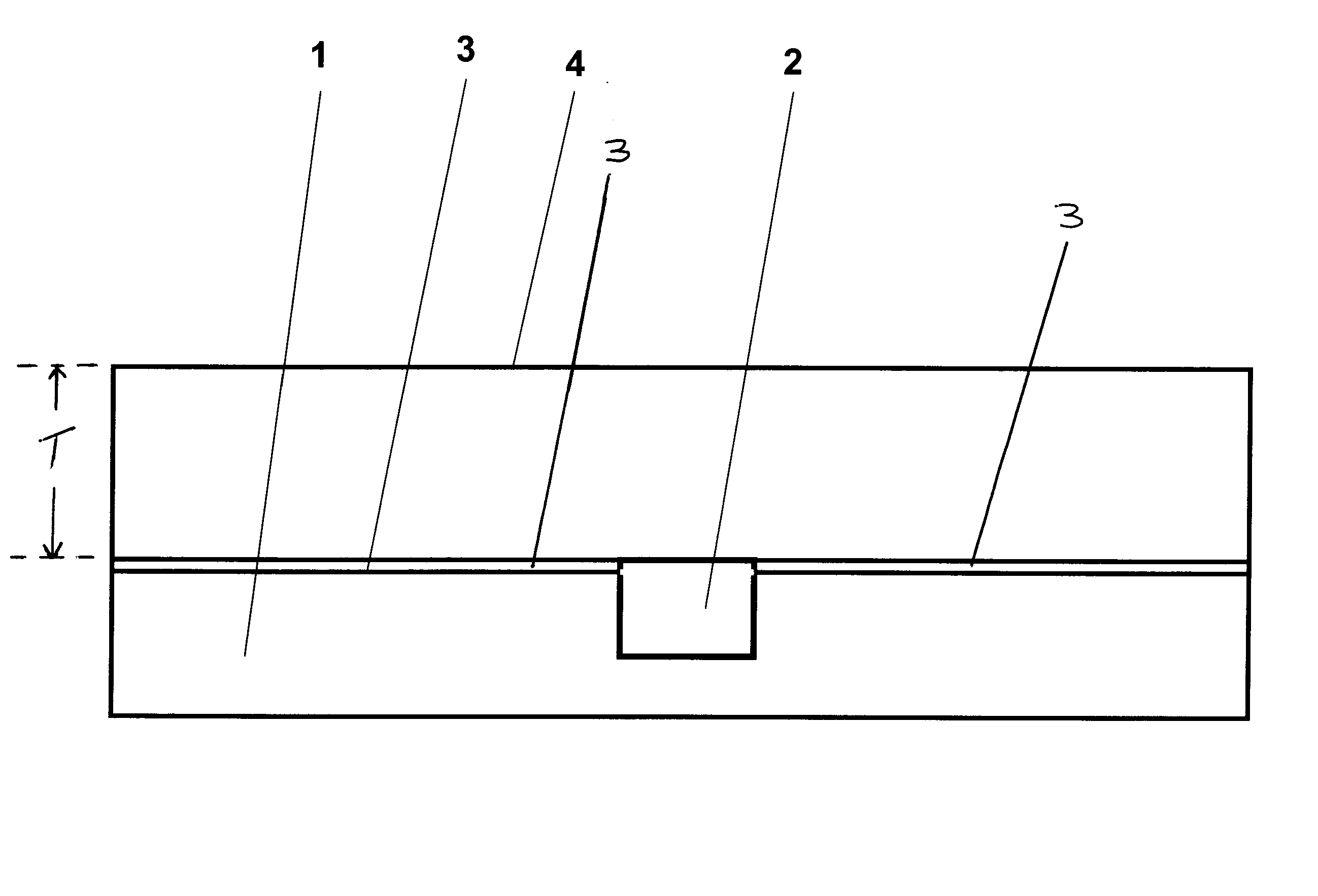
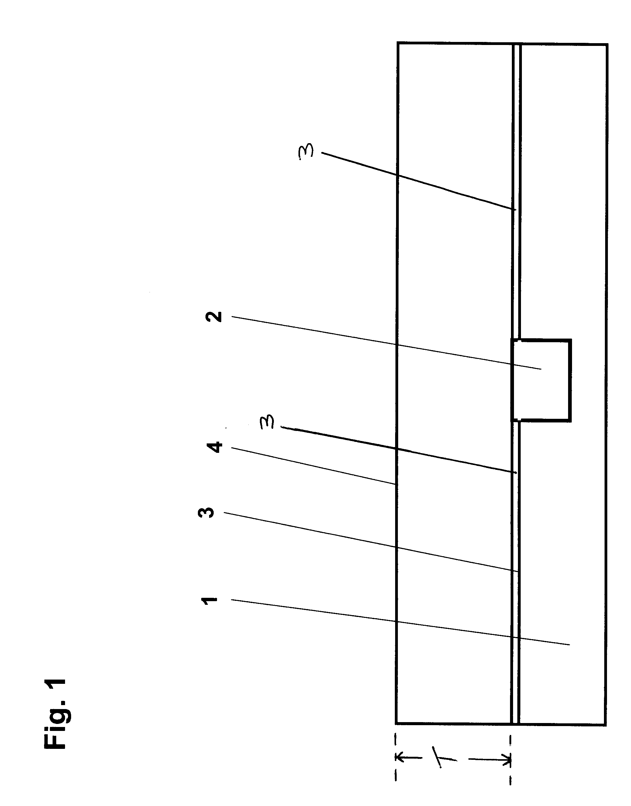
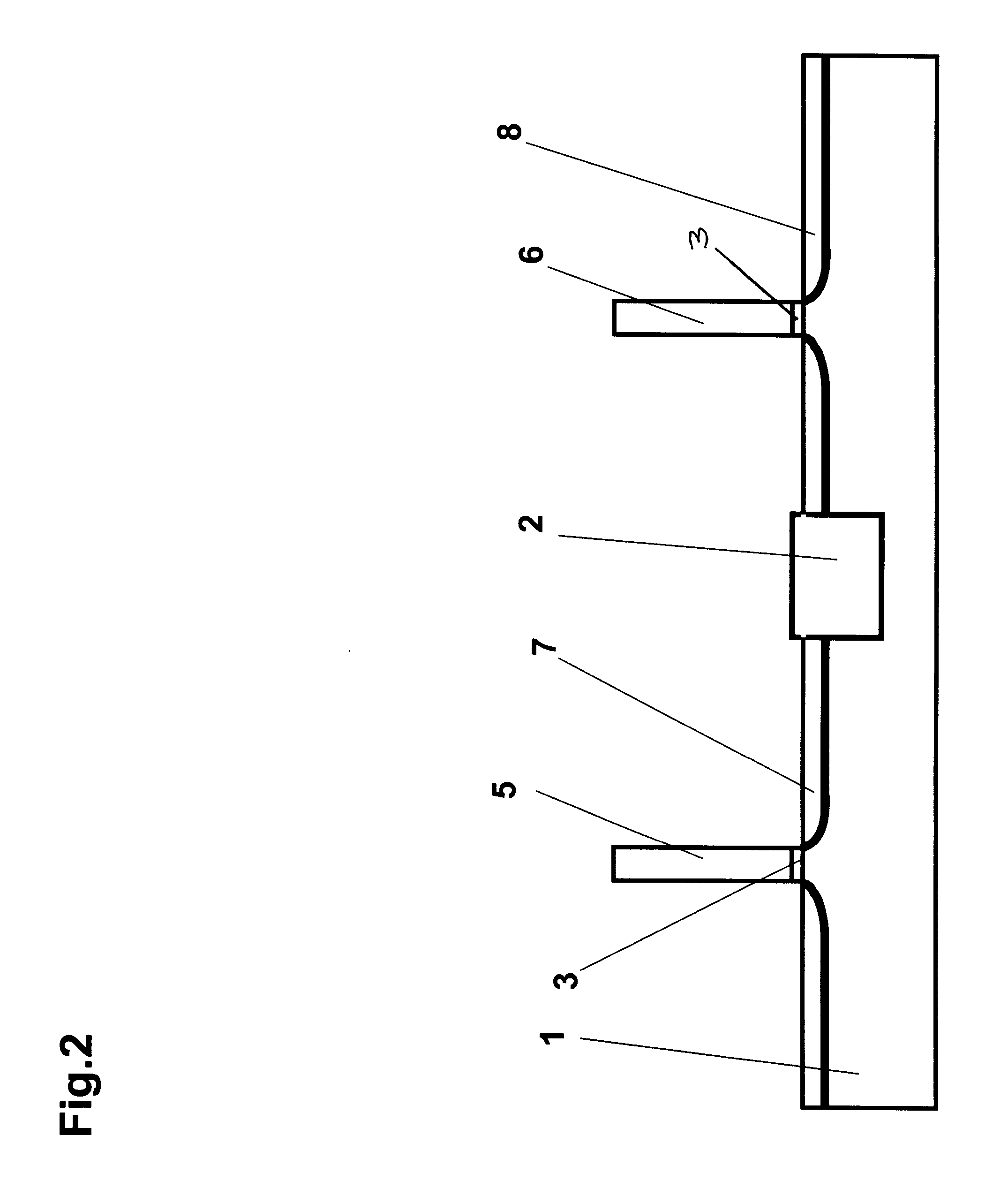
[0010] Turning now to the figures, and FIG. 1 in particular, a semiconductor substrate 1 is provided. The semiconductor substrate is a bulk Si substrate, an SOI substrate, or a stressed (strained) Si substrate. Alternatively, the substrate is a hybrid substrate which includes more than one surface orientation. The substrate alternatively includes a semiconductor material other than Si, such as Ge or any combination of Group III-V elements or Group II-V elements.
[0011] After an initial substrate cleaning procedure (conventional), an isolation scheme is carried out. As is well known in semiconductor manufacturing, the isolation scheme is used to separate selected devices electrically from each other. The isolation scheme may be a standard or a modified shallow trench isolation (STI) scheme. The STI 2 is shown in FIG. 1. Alternatively, the isolation is accomplished using a LOCOS process or mesa isolation scheme, as is well known in the art of fabricating semiconductor devices. For var...
PUM
 Abstract
Description
Claims
Application Information