Semiconductor integrated circuit device including dummy patterns located to reduce dishing

a technology of integrated circuits and dummy patterns, which is applied in the direction of superconductor devices, semiconductor/solid-state device testing/measurement, instruments, etc., can solve the problems of reducing the flatness of the product region, unable to completely eliminate dishing, etc., and achieves the reduction of the area over which dishing occurs, the effect of reducing the pattern interval and reducing the depth of the depression

Inactive Publication Date: 2005-05-26
RENESAS ELECTRONICS CORP
View PDF30 Cites 29 Cited by
  • Summary
  • Abstract
  • Description
  • Claims
  • Application Information

AI Technical Summary

Benefits of technology

[0007] By disposing a dummy pattern in a region where there is a large distance between patterns, so as to decrease the pattern interval, it is possible to deal with the problem of dishing (depressions) or undulations over a wide area. In dishing, the larger the area is the lower the position of the depression in the central part is; and, therefore, by disposing the dummy pattern so as to decrease the area over which dishing occurs, the depth of the depression can be relatively decreased.

Problems solved by technology

Nevertheless, no matter how small the pattern interval is made, dishing cannot be completely eliminated.
However, the dishing in the scribe region also affects the product region, and since the tolerance of focal depth in the exposure step is becoming more critical due to the trend towards higher detail, the decreased flatness of the product region (in particular the periphery) is a matter of concern.

Method used


Image

  • Semiconductor integrated circuit device including dummy patterns located to reduce dishing
  • Semiconductor integrated circuit device including dummy patterns located to reduce dishing
  • Semiconductor integrated circuit device including dummy patterns located to reduce dishing

Examples


Embodiment Construction

[0060] One embodiment of this invention will now be described in detail with reference to the drawings. In all of the drawings which illustrate this embodiment, the same symbols are used for members having identical functions, and their description will not be repeated.

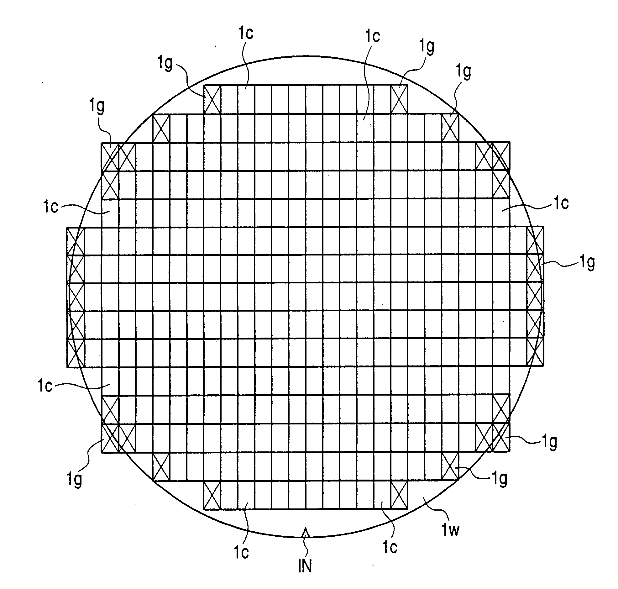
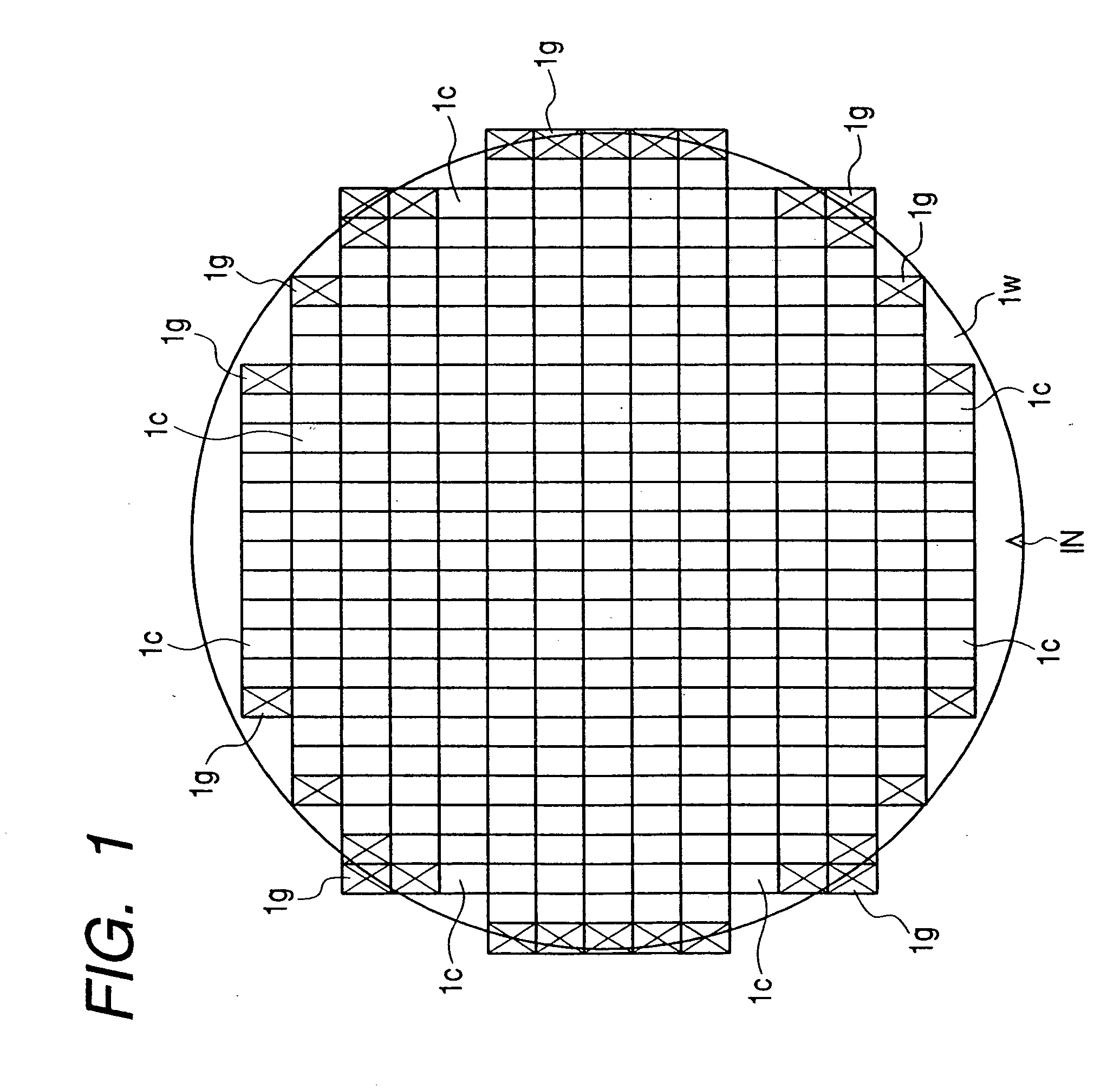
[0061]FIG. 1 is a plan view showing a silicon wafer used for manufacturing a semiconductor integrated circuit device according to one embodiment of the invention. A notch In is made in a single crystal silicon wafer 1w and serves as a crystal plane index mark of the wafer 1w. A chip 1c is formed on the wafer 1w. The chip 1c is formed in the effective processing area of the wafer 1w, and a chip region 1g outside the effective processing area is not used.

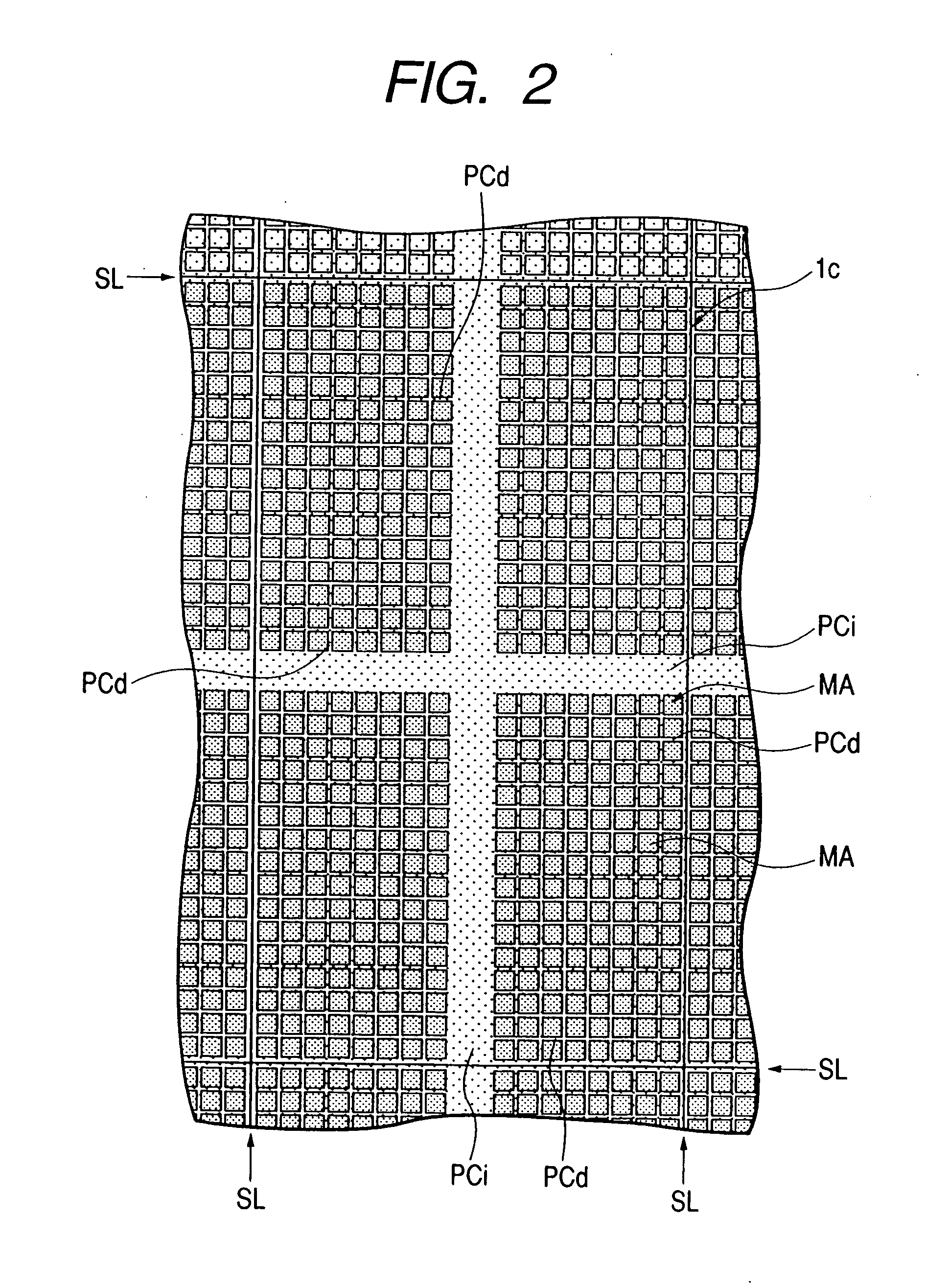
[0062]FIG. 2 is a plan view showing an enlargement of the chip 1c of the wafer 1w. The chip 1c is scribed and divided by a scribe line SL. In the steps described hereafter, each step is performed in the state of the wafer 1w, the chip 1c being divided in the final ste...


PUM


Abstract

A large area dummy pattern DL is formed in a layer underneath a target T2 region formed in a scribe region SR of a wafer. A small area dummy pattern in a lower layer and a small area dummy pattern Ds2 in an upper layer are disposed in a region where the inter-pattern space of a pattern (active regions L1, L2, L3, gate electrode 17), which functions as an element of a product region PR and scribe region SR, is wide. The small area dummy pattern Ds2 in the upper layer is offset by ½ pitch relative to the small area dummy pattern Ds in the lower layer.

Description

CROSS REFERENCE TO RELATED APPLICATION [0001] This is a continuation of U.S. application Ser. No. 09 / 692,450, filed Oct. 20, 2000, the subject matter of which is incorporated by reference herein.BACKGROUND OF THE INVENTION [0002] This invention relates to a semiconductor integrated circuit device and to a process for manufacturing the same; and, in particular, the invention relates to a process which can effectively be applied to a semiconductor integrated circuit device comprising a step for flattening a surface using CMP (Chemical Mechanical Polishing). [0003] In semiconductor integrated circuit devices, such as a DRAM (Dynamic Random Access Memory), demand has been increasing in recent years for finer detail and a higher degree of integration. Due to the demand for greater detail in semiconductor integrated circuit devices, laminated structures in multilayer interconnections are unavoidable, but if a multilayer structure is used, imperfections are formed on the surface of the upp...

Claims


Application Information

Patent Timeline
Patent Type & Authority Applications(United States)
IPC IPC(8): H01L21/76H01L21/302H01L21/304H01L21/3105H01L21/3205H01L21/762H01L21/768H01L23/52H01L23/544
CPCG03F9/7076H01L21/31053H01L21/76229H01L21/76819H01L22/34H01L23/544H01L23/585H01L2924/0002H01L2223/54453H01L21/30625H01L21/78H01L2924/00H01L21/302H01L27/0207H01L29/78
Inventor UCHIYAMA, HIROYUKICHAKIHARA, HIRAKUICHISE, TERUHISAKAMINAGA, MICHIMOTO
Owner RENESAS ELECTRONICS CORP
Why Eureka
Try Eureka