
Adaptive delay control circuit for switched mode power supply

a control circuit and switching mode technology, applied in the direction of instrumentation, process and machine control, pulse technique, etc., can solve the problems of reducing the conversion efficiency of the power supply, causing long dead times during which neither switch is conducting, and damage to the switch, so as to prevent the cross-conduction of the high and minimize the dead times between switch transitions

Active Publication Date: 2005-05-26
BEL POWER SOLUTIONS INC
View PDF29 Cites 53 Cited by
  • Summary
  • Abstract
  • Description
  • Claims
  • Application Information

AI Technical Summary

Benefits of technology

[0009] The present invention satisfies the need for an adaptive delay control for a switched mode power supply that prevents cross conduction of the high and low side switches while also minimizing the dead times between switch transitions.
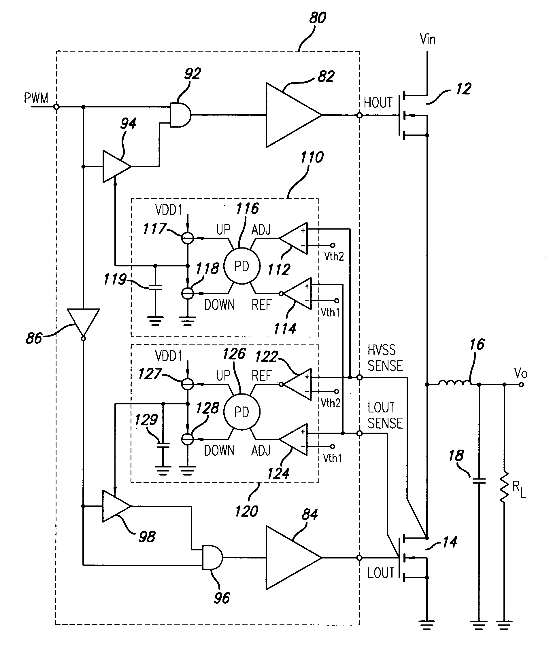
[0010] In an embodiment of the invention, a switched mode power supply comprises a first switch coupled to an input power source, a second switch coupled to ground, and an output filter coupled to a phase node defined between the first and second switches. The first and second switches are responsive to a pulse width modulated signal to thereby regulate power provided to the output filter. A feedback loop monitors operation of the first and second switches and delays activation of one of the first and second switches to preclude simultaneous conduction and minimize dead time between state transitions of the first and second switches. The feedback loop comprises at least one delay control circuit adapted to delay delivery of the pulse width modulated signal to at least one of the first and second switches. The delay control circuit detects a phase difference between state transitions of the first and second switches and provides a delay corresponding to a magnitude of the phase difference.

Problems solved by technology

This would short the positive supply voltage to ground through the high and low side switches, potentially damaging the switches and otherwise reducing the conversion efficiency of the power supply.
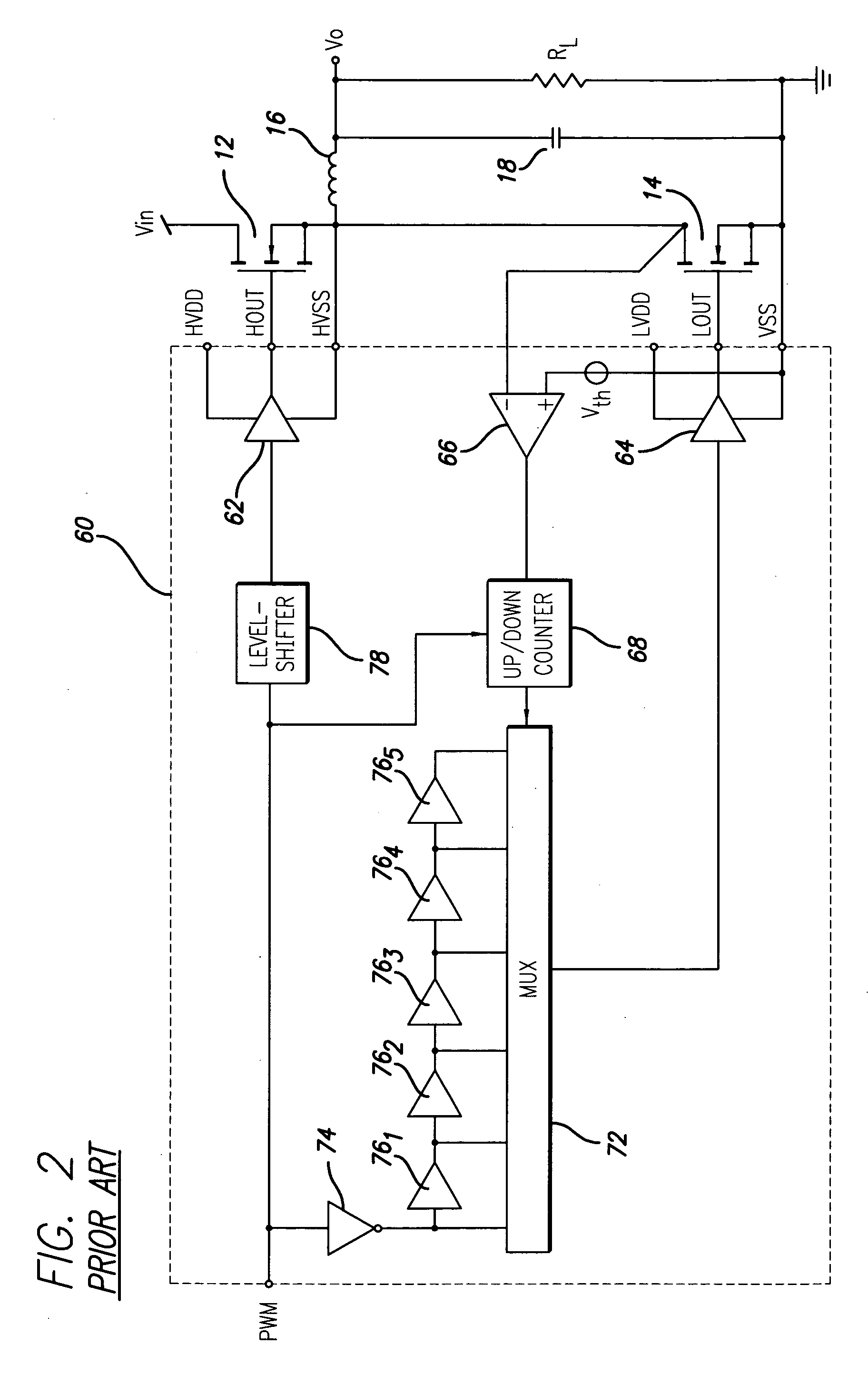
While this method prevents simultaneous conduction of the power switches, a drawback is that the time delays produce lengthy dead times during which neither switch is conducting.
The voltage drop across the body diode (or Shottky diode) tends to further reduce the conversion efficiency of the power supply.
Moreover, the method is only responsive to load changes and input voltage changes, but cannot compensate for varying propagation delays in the power supply circuit due to temperature changes or silicon process changes.
While this control method is adaptive, the quantized delay is not “quiet” since the delay line will often bounce between two adjacent delay settings, thereby introducing noise in the pulse width modulation signal and hence the output voltage of the power supply.
Moreover it is difficult to sense the drain-source voltage of the low side switch in order to detect the starting point of body diode conduction because of parasitic inductances.
An inaccurate measurement of the zero voltage transition will affect the operation of the control loop.

Method used


Image

  • Adaptive delay control circuit for switched mode power supply
  • Adaptive delay control circuit for switched mode power supply
  • Adaptive delay control circuit for switched mode power supply

Examples


Embodiment Construction

[0019] The present invention provides an adaptive delay control for a switched mode power supply that prevents cross conduction of the high and low side switches while also minimizing the dead times between switch transitions. In the detailed description that follows, like element numerals are used to describe like elements illustrated in one or more figures.

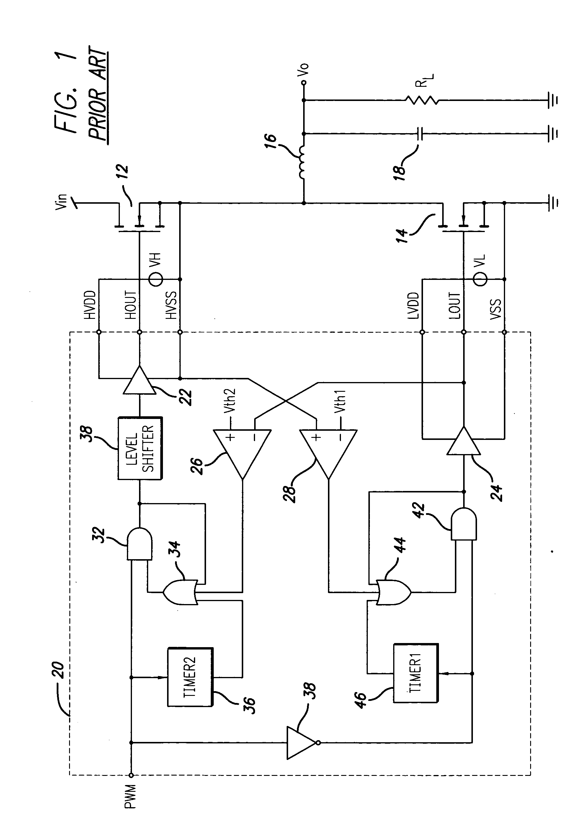
[0020] Referring first to FIG. 1, an example of a conventional delay control circuit for a switched mode power supply is shown. The power supply comprises a buck converter topology used to convert an input DC voltage Vin to an output DC voltage Vo applied to a resistive load (RL). The input DC voltage Vin may further comprise an output of a galvanic isolation transformer of a DC-to-DC converter. The power supply includes high side switch 12, low side switch 14, output inductor 16, and capacitor 18. The drain terminal of the high side switch 12 is coupled to the input voltage Vin, the source terminal of the low side switch 14 is...


PUM


Abstract

A switched mode power supply comprises a first switch coupled to an input power source, a second switch coupled to ground, and an output filter coupled to a phase node defined between the first and second switches. The first and second switches are responsive to a pulse width modulated signal to thereby regulate power provided to the output filter. A controller is provided in a feedback loop that monitors operation of the first and second switches and delays activation of one of the first and second switches to preclude simultaneous conduction. The controller comprises at least one delay control circuit adapted to delay delivery of the pulse width modulated signal to at least one of the first and second switches. The delay control circuit detects a phase difference between state transitions of the first and second switches and provides a delay corresponding to a magnitude of the phase difference.

Description

BACKGROUND OF THE INVENTION [0001] 1. Field of the Invention [0002] The present invention relates to switched mode power supplies, and more particularly to a pulse width modulation control circuit for a switched mode power supply that provides adaptive delay control to prevent cross-conduction of high and low side switches during switch state transitions. [0003] 2. Description of Related Art [0004] Switched mode power supplies are known in the art to convert an available direct current (DC) level voltage to another DC level voltage. A buck converter is one particular type of switched mode power supply that delivers a regulated DC output voltage to a load by selectively storing energy in an output inductor coupled to the load by switching the flow of current into the output inductor. The buck converter includes two power switches, referred to as high side and low side switches, that are typically provided by MOSFET transistors. The high side switch couples the output inductor to a po...

Claims


Application Information

Patent Timeline
IPC IPC(8): H02M1/00G05F1/40H02MH02M1/38H02M3/158
CPCH02M1/38H02M3/1588H03K17/165Y02B70/10G05F1/40H02M3/28
Inventor CHAPUIS, ALAIN
Owner BEL POWER SOLUTIONS INC
Learn More