Laser irradiation apparatus and method for manufacturing semiconductor device

Inactive Publication Date: 2005-05-26
SEMICON ENERGY LAB CO LTD
View PDF8 Cites 32 Cited by
  • Summary
  • Abstract
  • Description
  • Claims
  • Application Information

AI Technical Summary

Problems solved by technology

This is because an inexpensive glass substrate, which is often employed as a substrate of TFT, is inferior in heat resistance and is easy to change in shape due to the heat.
However, when the cylindrical lens transfers the image having homogeneous intensity distribution to the irradiated surface, the homogeneity of the intensity distribution of the beam spot formed on the irradiated surface is adversely affected by the aberration. FIG. 2 is an enlarged view of a structure in which the intensity distribution of the

Method used


Image

  • Laser irradiation apparatus and method for manufacturing semiconductor device
  • Laser irradiation apparatus and method for manufacturing semiconductor device
  • Laser irradiation apparatus and method for manufacturing semiconductor device

Examples


embodiment 1

[0048] [Embodiment 1]

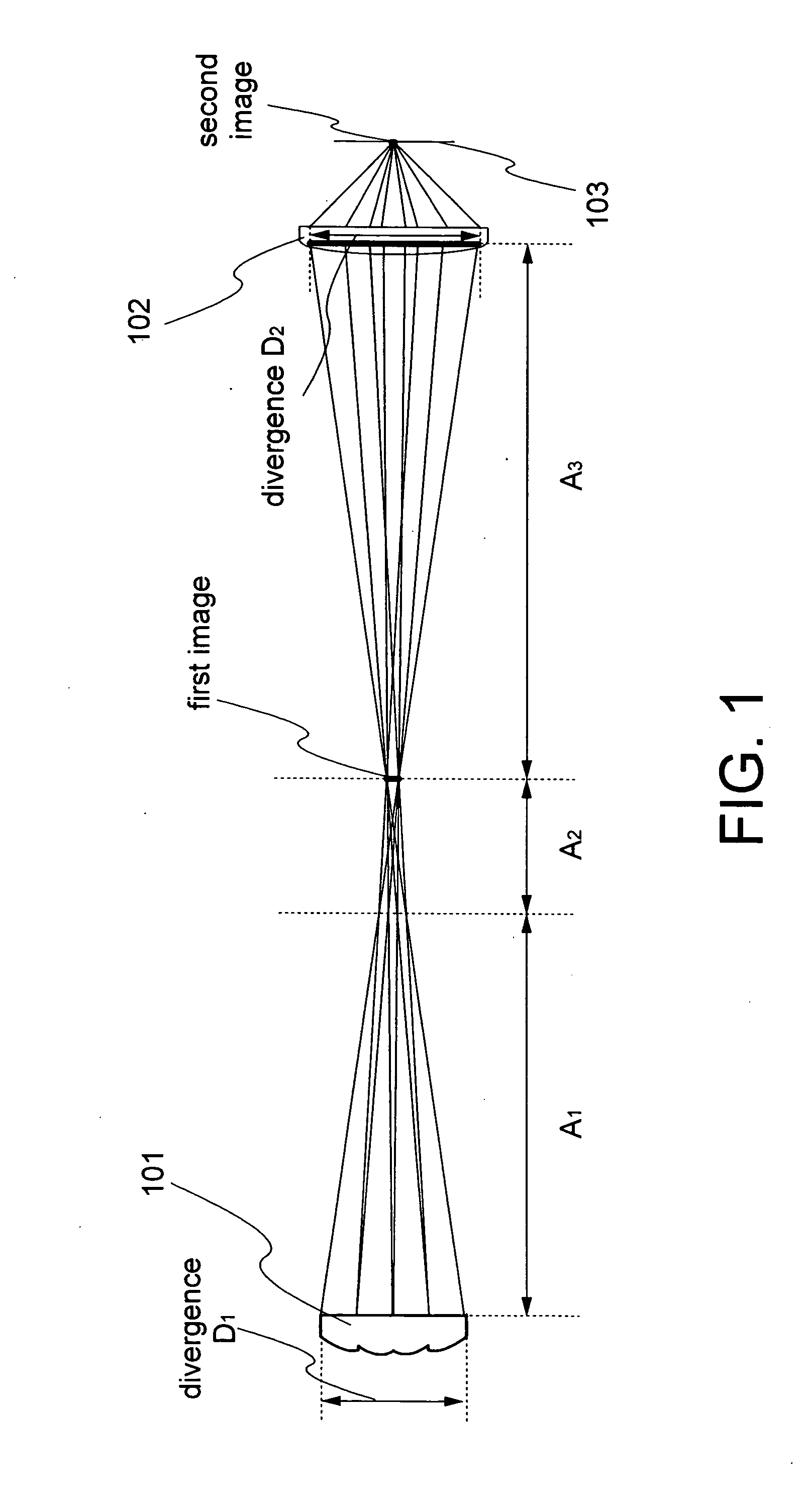
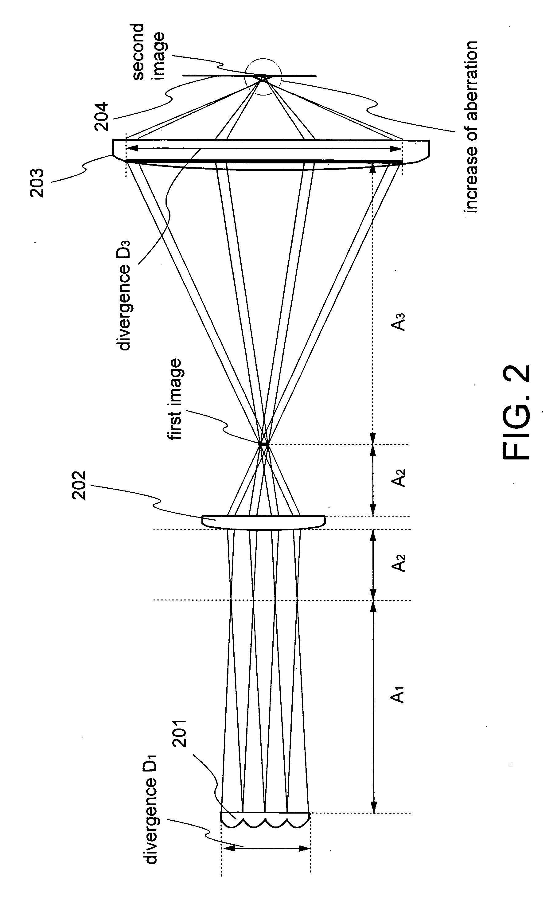
[0049] This embodiment explains in detail a condition of the optical system described in the embodiment mode of the present invention. Moreover, the present embodiment explains a laser irradiation apparatus using the optical system with reference to FIGS. 3A and 3B.

[0050] In a side view of FIG. 3A, an example is explained in which the intensity distribution of a linear beam formed on an irradiated surface 305 is homogenized in a direction of a short side of the linear beam using an off-axis cylindrical lens array and a cylindrical lens. Moreover, in a top view of FIG. 3B, an example is explained in which the intensity distribution of the linear beam is homogenized in a direction of its long side using another off-axis cylindrical lens array. An excimer laser is used as the laser oscillator 301. A laser beam emitted from the laser oscillator 301 propagates in a direction indicated by an arrow and is irradiated to the irradiated surface 305 after transmitting thr...

embodiment 2

[0054] [Embodiment 2]

[0055] The present embodiment explains an example of the laser irradiation apparatus of the present invention using a light pipe with reference to FIG. 4.

[0056] In FIG. 4, a laser oscillator 401 is an excimer laser. Reference numerals 402 and 403 denote off-axis cylindrical lens arrays. A light pipe 404 has a pair of reflection planes provided oppositely, which is set so as to act on a direction of a short side of a linear beam spot formed on an irradiated surface 406. The space between the pair of reflection planes is 2 mm. In FIG. 4A, the direction of the short side of the linear beam spot formed on the irradiated surface 406 is parallel to the paper. The space between the pair of reflection planes of the light pipe 404 is filled with the air. The laser beam incident into the light pipe 404 is reflected inside the light pipe 404 repeatedly and the divided laser beams are superposed on the same plane. Thus, the intensity distribution of the laser beam is homog...

embodiment 3

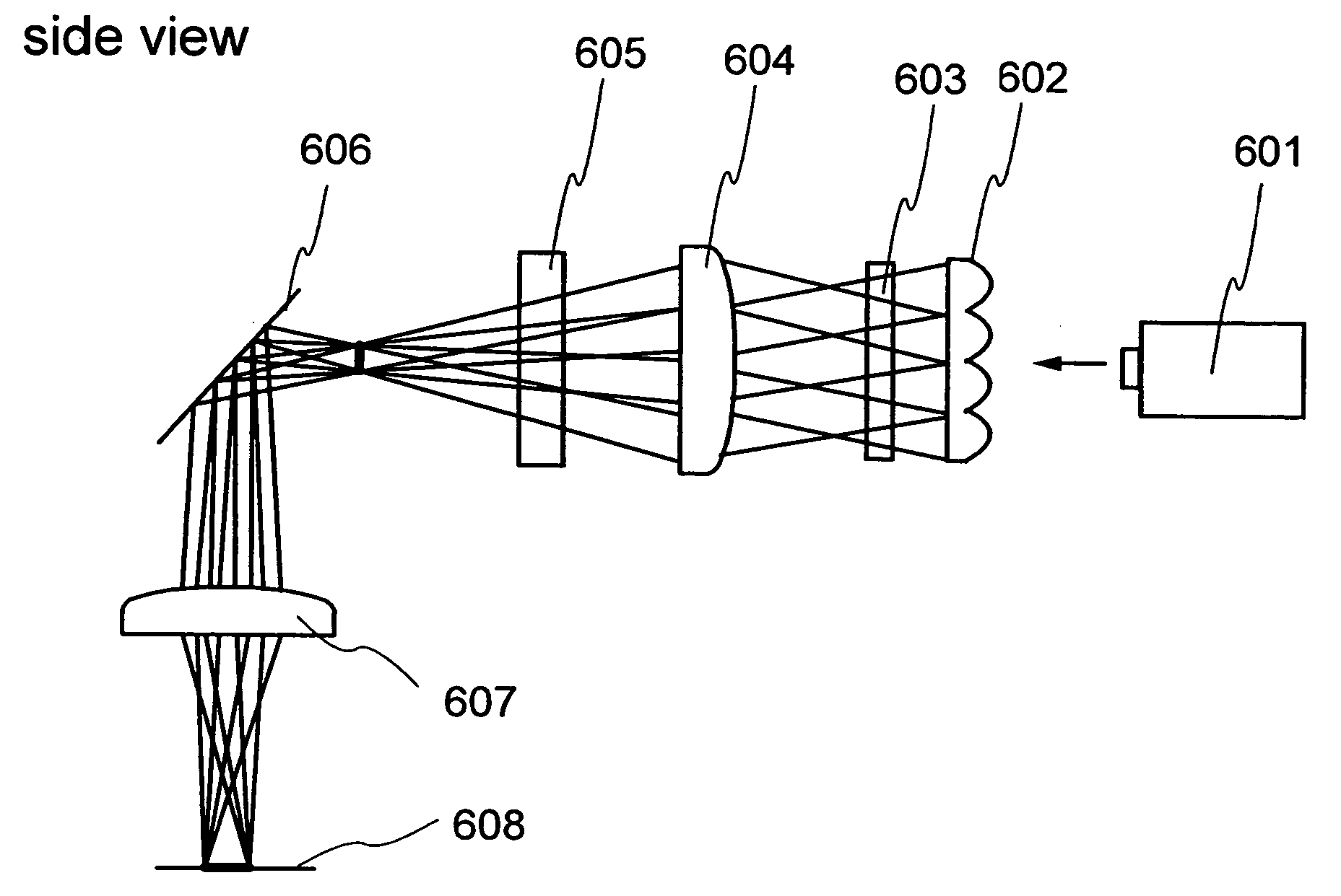
[0062] [Embodiment 3]

[0063] The present embodiment explains an example of a laser irradiation apparatus using the off-axis cylindrical lens array of the present invention in combination with the conventional cylindrical lens array with reference to FIGS. 5A and 5B.

[0064] In a side view of FIG. 5A, a laser beam emitted from a laser oscillator 501 propagates in a direction indicated by an arrow. An off-axis cylindrical lens array 502 divides the laser beam into four, and the divided beams are superposed on a predetermined plane so that an image having homogeneous intensity distribution is formed on the predetermined plane. A cylindrical lens 505 positioned behind the image transfers the image to an irradiated surface 506. In FIG. 5A, a direction of a short side of the linear beam formed on the irradiated surface 506 is parallel to the paper. When the off-axis cylindrical lens array 502 is set so that it has curvature in the direction of the short side, the following advantage can be ...


PUM


Abstract

When a rectangular image having homogeneous intensity distribution is transferred by an imaging optical system, aberration adversely affects the homogeneity of the intensity distribution. The present invention provides a laser irradiation apparatus that can suppress the aberration due to the imaging optical system typified by a cylindrical lens, that can enlarge the square measure of the beam spot in which the intensity distribution is homogenous, and that can anneal the irradiated surface homogeneously efficiently. Moreover, the present invention provides a method for manufacturing a semiconductor device with the use of the laser irradiation apparatus. In the present invention, the divergence of the laser beam is suppressed and the size of the imaging optical system is miniaturized by using an off-axis lens array such as an off-axis cylindrical lens array. By the miniaturization, it is possible to reduce the cost, to facilitate the maintenance, and to suppress the aberration. By suppressing the aberration, the homogeneity of the intensity distribution of the beam spot can be improved.

Description

BACKGROUND OF THE INVENTION [0001] 1. Field of the Invention [0002] The present invention relates to a laser irradiation apparatus and a method for manufacturing a semiconductor device with the use of the laser irradiation apparatus. [0003] 2. Description of the Related Art [0004] In recent years, a technique to form a thin film transistor (hereinafter referred to as a TFT) over a substrate has made great progress, and application development to an active matrix display device has been advanced. Particularly, a TFT formed using a poly-crystalline semiconductor film is superior in field-effect mobility to a TFT formed using a conventional amorphous semiconductor film, and therefore high-speed operation becomes possible when the TFT is formed using the poly-crystalline semiconductor film. For this reason, a circuit for driving a pixel, which has been mounted by an external IC chip, can be formed integrally with the pixel over the same substrate by the TFT. [0005] The poly-crystalline ...

Claims


Application Information

Patent Timeline
IPC IPC(8): G02B27/09
CPCG02B27/0966G02B19/0014G02B19/0052
Inventor TANAKA, KOICHIRO
Owner SEMICON ENERGY LAB CO LTD
Why Eureka
Try Eureka