

Seamless holographic embossing substrate produced by laser ablation
a technology of laser ablation and embossing substrate, which is applied in the direction of substrates with holograms, photomechanical treatment, instruments, etc., can solve the problems of difficult to eliminate the shim line in the final embossed product, the above described methods are often confined, and the embossed holographic image breaks
- Summary
- Abstract
- Description
- Claims
- Application Information
AI Technical Summary
Benefits of technology
Problems solved by technology
Method used
Image

Examples
Embodiment Construction
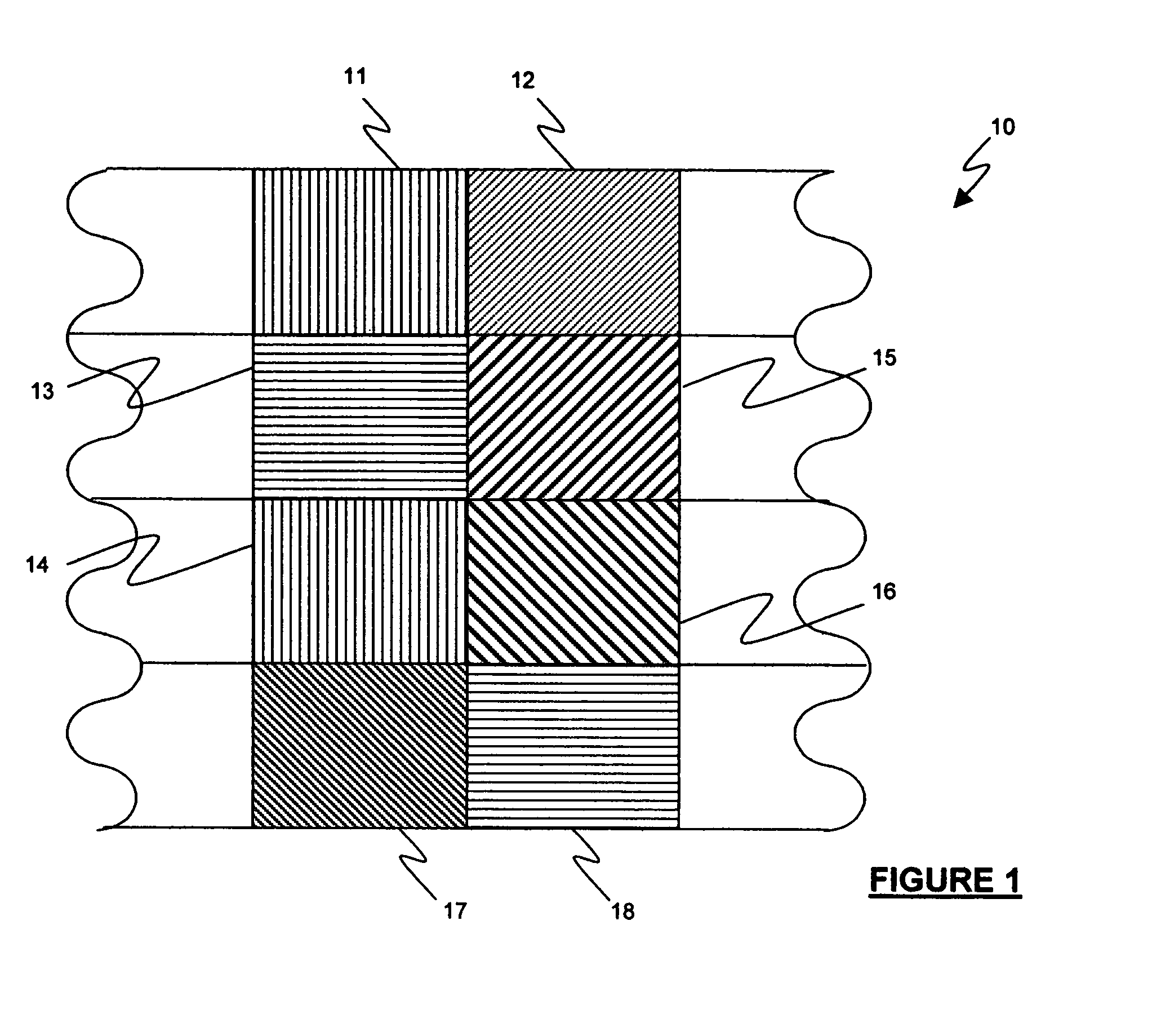
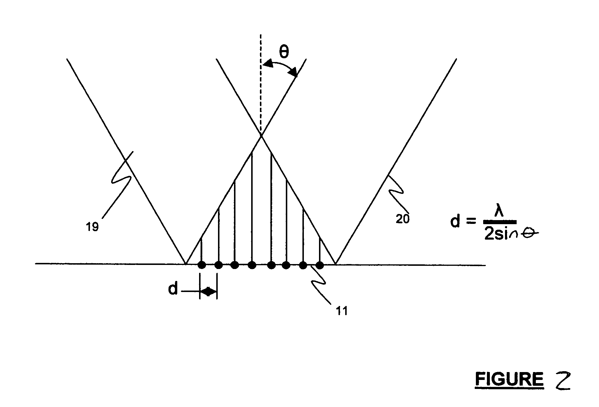
[0022] Provided in FIG. 1 is an illustrative portion 10 of a seamless substrate of the present invention with enlarged views of diffraction gratings in several pixels (11-18) ablated by interfering laser beams. In particular, shown in FIG. 1 are diffraction gratings of different pitches (a grating pitch can be defined as a distance between the adjacent crests or grooves), and different orientations of the grooves or crests relative to some direction. Each diffraction grating in each pixel is created by interfering two laser beams 19 and 20 on the surface of the seamless substrate, as shown in FIG. 2 with regard to pixel 11. The interfering laser beams 19 and 20 form an interference pattern characterized by a number of periodic maxima and minima in the laser intensity with a period (pitch) d. Period d is defined by the diffraction equation as d=λ / 2 sinθ. The intensity maxima have sufficient energy to ablate the material of a substrate 60 at pixel 11 and form a diffraction grating 25 ...
PUM
 Abstract
Description
Claims
Application Information