System and method for removal of photoresist in transistor fabrication for integrated circuit manufacturing

a technology of photoresist and integrated circuit, which is applied in the field of system and method for removing photoresist in frontend fabrication, can solve the problems of insufficient thickness of critical layers on the wafer surface, inability to meet all process requirements, and inability to strip crust in pure oxygen. the effect of reducing the thickness of critical layers

Active Publication Date: 2005-05-26
MATTSON TECHNOLOGY +1
View PDF27 Cites 30 Cited by
  • Summary
  • Abstract
  • Description
  • Claims
  • Application Information

AI Technical Summary

Benefits of technology

[0018] A method is disclosed for use in a system which is configured for fabricating an integrated circuit on one or more workpieces. The system includes a front end that is operable at an ambient pressure for use in moving the workpieces, at least portions of which support a photoresist layer, into and out of the system and for removing the photoresist in a process chamber at a process pressure. The process pressure being less than the ambient pressure. The system includes a front end robot for moving the workpieces into and out of the system. In one aspect of the disclosure, the method includes configuring a first chamber to serve as a loadlock, in selective communication with the front end. A second chamber is arranged in selective communication with each of the first chamber and with the process chamber. A workpiece transfer arrangement is located in the second chamber for cooperating with the front end robot to transfer the workpieces between the front end and the process chamber in sequence through the first chamber and the second chamber such that the second chamber is isolated from the ambient pressure at all times during transfer of workpieces between the front end and the process chamber. A gas flow arrangement is connected to a plasma source to serve in providing a gas flow to the plasma source during a treatment process such that the plasma source produces reactive species from hydrogen, as a principal source of ...

Problems solved by technology

It is submitted that current PR stripping processes for these applications will become inadequate to meet all process requirements in the near future as the size of transistors continues to shrink and the thickness of critical layers on the wafer surface continues to decrease.
Otherwise the stripping of crust in pure oxygen is often so slow that the cost is prohibitively high.
Such methods, however, still do not yield fast and highly productive etching of the crust.
However, the stripping of the bulk photoresist is not normally the final step, due to the significant side-effects of ion implantation.
Very often, there are difficult to remove residues remaining after removing most of the crust and all the bulk PR.
Unfortunately, fluorine-containing gas addition has been shown in high temperature stripping processes to attack the gate dielectric—typically silicon dioxide or oxynitride.
The potential vulnerability of the gate and gate dielectric materials to the stripping process will likely increase as technology advances, due to the decreasing length of the gate which is typically about half the size of other critical features patterned on the wafer.
Unfortun...

Method used


Image

  • System and method for removal of photoresist in transistor fabrication for integrated circuit manufacturing
  • System and method for removal of photoresist in transistor fabrication for integrated circuit manufacturing
  • System and method for removal of photoresist in transistor fabrication for integrated circuit manufacturing

Examples


Embodiment Construction

[0028] The following description is presented to enable one of ordinary skill in the art to make and use the invention and is provided in the context of a patent application and its requirements. Various modifications to the described embodiments will be readily apparent to those skilled in the art and the generic principles herein may be applied to other embodiments. Thus, the present invention is not intended to be limited to the embodiment shown but is to be accorded the widest scope consistent with the principles and features described herein. It is noted that the drawings are not to scale and are diagrammatic in nature.

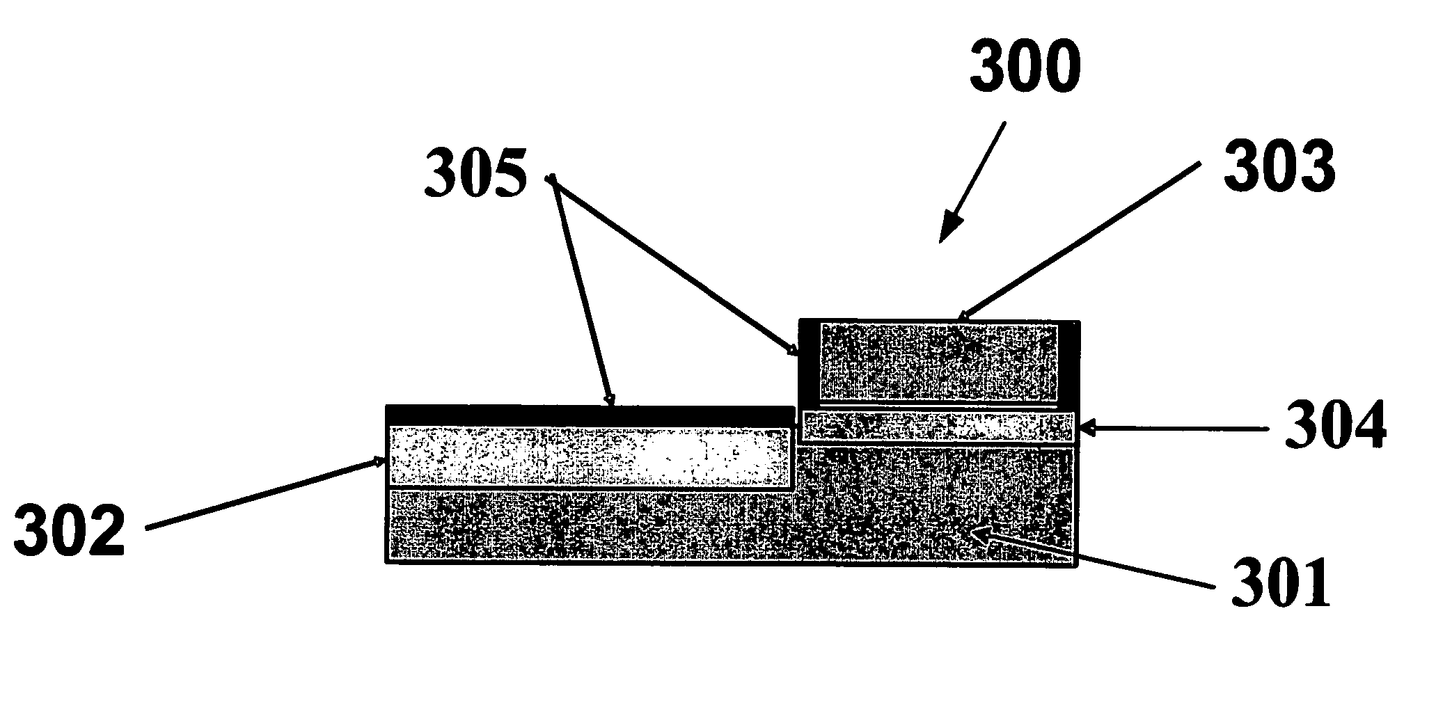
[0029] It is recognized that, for purposes of current and future IC fabrication, there are serious concerns with respect to the integrity of the very thin layers—typically between 100 Angstroms and 300 Angstroms—to be used for junctions and for protective layers. As a side-effect, RIE, in addition to the difficulties which accompany its use such as discussed abo...


PUM


Abstract

In a technique for fabricating an integrated circuit to include an active device structure which supports an electrical interconnect structure, a photoresist layer is used prior to forming an electrical interconnect structure on the active device structure. The photoresist and related residues are removed by exposing the photoresist and exposed regions of the active device structure to one or more reactive species that are generated using a gas mixture including hydrogen gas, as a predominant source of the reactive species, in a plasma source such that the photoresist and residues are continuously exposed to hydrogen-based reactive species. An associated system architecture is described which provides for a substantial flow of hydrogen gas in the process chamber.

Description

RELATED APPLICATION [0001] The present application claims priority from U.S. Provisional Application Ser. No. 60 / 511,029 filed on Oct. 13, 2003, which is incorporated herein by reference.BACKGROUND OF THE INVENTION [0002] The present invention is related generally to semiconductor fabrication and, more particularly, to a system and method for removal of photoresist in front-end fabrication as part of integrated circuit manufacturing. [0003] A schematic of a standard configuration of a photoresist (PR) stripping chamber and source is shown in FIG. 1. Gas coming from a set of flow controllers and valves 101, passes via tubing 102 to a plasma source 103. There, the gas becomes substantially dissociated (and partially ionized) and then goes through a distribution / baffling system 104 into a wafer process enclosure 105. A pedestal 106 holds a wafer 107 which is to be stripped of PR and residues. On the wafer, radicals react with the PR and residues to form volatile or water-soluble reacti...

Claims


Application Information

Patent Timeline
IPC IPC(8): H01LH01L21/00H01L21/02H01L21/302H01L21/311H01L21/461
CPCH01L21/02063H01L21/67207H01L21/31138H01L21/02071
Inventor SAVAS, STEPHEN E.XU, SONGLINDUTTON, DAVIDKADAVANICH, ANDREASGEORGE, RENE
Owner MATTSON TECHNOLOGY
Why Eureka
Try Eureka