On-wafer monitoring system

a monitoring system and micro-nano technology, applied in the direction of resistance/reactance/impedence, semiconductor/solid-state device testing/measurement, instruments, etc., can solve the problems of large disturbance in plasma, inability to accurately measure incident particles, and virtually impossible actual measurement of in-service plasma treatment devices

Inactive Publication Date: 2005-06-02
TOHOKU TECHNO ARCH CO LTD
View PDF10 Cites 35 Cited by
  • Summary
  • Abstract
  • Description
  • Claims
  • Application Information

AI Technical Summary

Problems solved by technology

In the conventional method, the size of the pinholes is about a few mm that is in an entirely different value from actual processing dimensions, and thus it was impossible to accurately measure the incident particles.
Further, a differential exhaust system has been required to restrict the changes of energy and charge state caused by the collision among particles in an analyzer tube of an energy analyzer, and the actual measurement on an in-service plasma treatment device was virtually impossible.
As described, a conventional plasma measurement system has a large and complicate apparatus (probe, mass spectrometer, and the like) and causes large disturbance in plasma.
In addition, since the cost of apparatus was expensive and so on, it has been difficult to apply it to an actual production apparatus.

Method used


Image

  • On-wafer monitoring system
  • On-wafer monitoring system
  • On-wafer monitoring system

Examples


Embodiment Construction

[0037] The embodiments of the present invention will be described in detail with reference to the drawings.

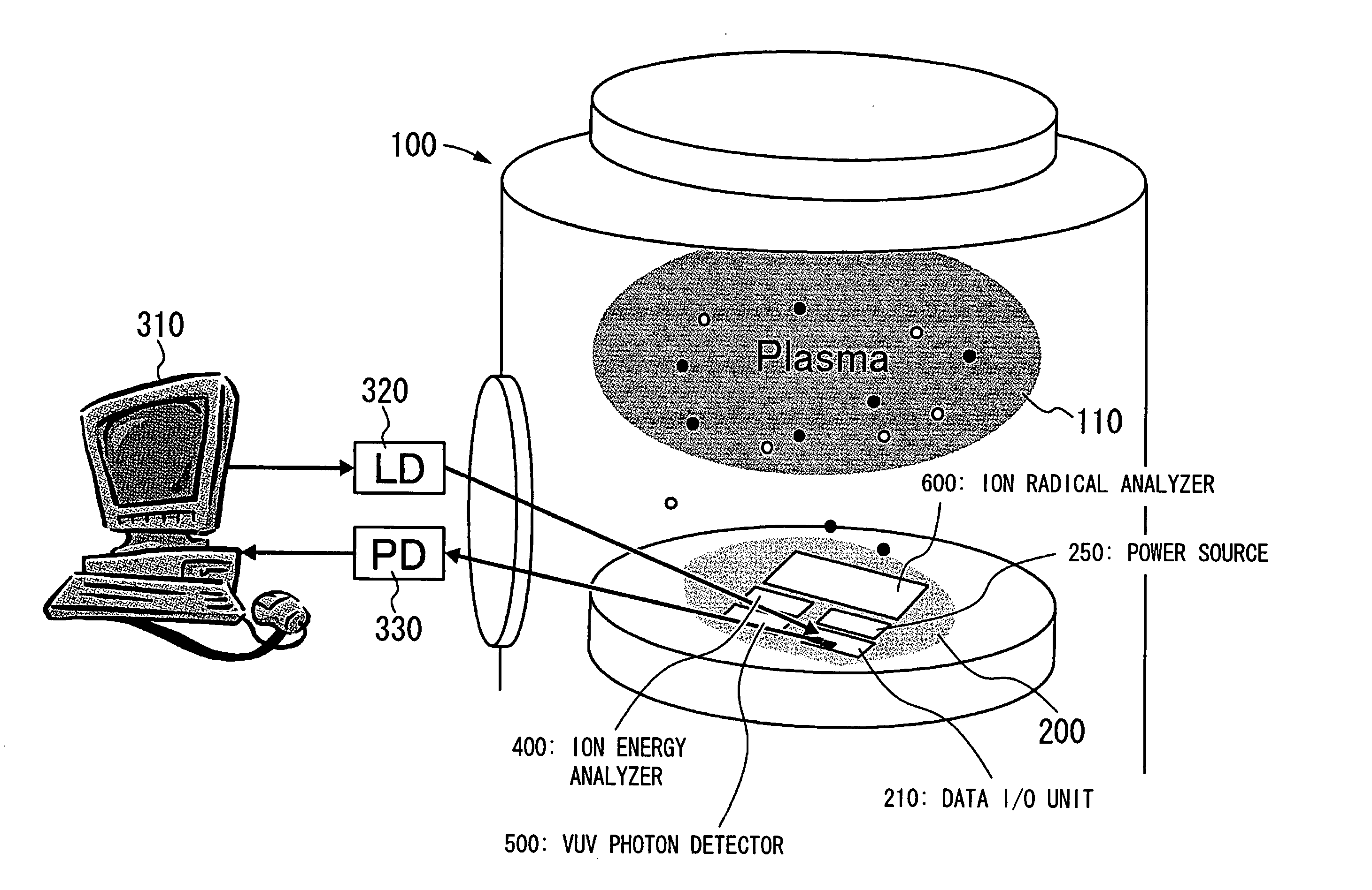
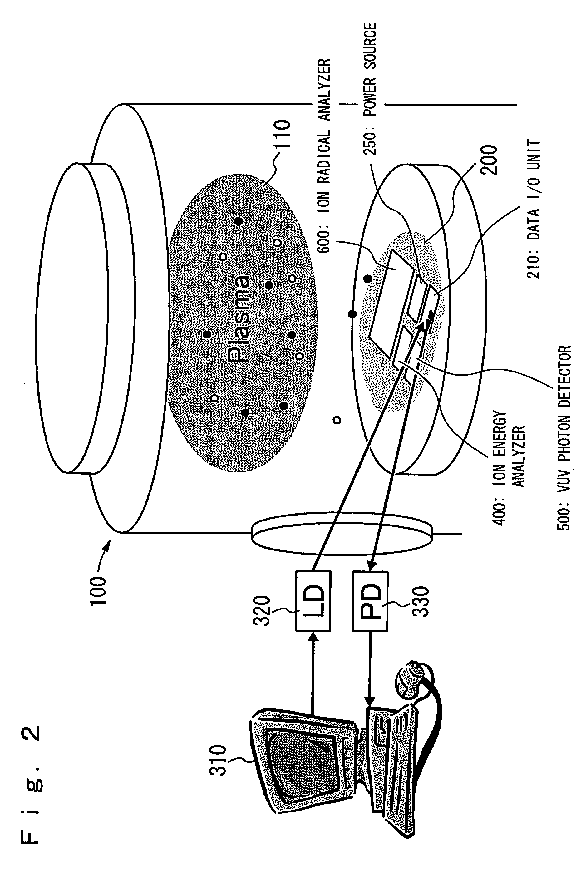
[0038]FIG. 2 and FIG. 3 show the basic structure of the on-wafer monitoring system according to the present invention.

[0039]FIG. 2 shows the on-wafer monitoring system 200 where sensors and the like are created on a substrate and placed on the position of a substrate to be treated in the plasma treatment device 100. The on-wafer monitoring system 200, as shown in FIG. 3, comprises various kinds of sensors which are created on the substrate, a data I / O unit 210 that inputs / outputs data from / to outside via light, and a power source unit 250 that supplies power source to them. The on-wafer data I / O unit 210 is connected to a laser diode (LD) 320 and a photo diode (PD) 330, which are I / O units via light installed outside, and it receives instructions from outside and transmits monitored data to the outside.

[0040] The on-wafer monitoring system 200 shown in FIG. 2 and FIG. 3 is a...


PUM

PropertyMeasurementUnit
energyaaaaaaaaaa
sizeaaaaaaaaaa
sizeaaaaaaaaaa

Abstract

An on-wafer monitoring system (200) is placed at a position of a substrate to be treated in a plasma treatment device (100). The on-wafer monitoring system (200) includes various sensors, a data I / O unit (210) for optically inputting / outputting data to / from outside, and an internal power source unit (250) for supplying power to them. The on-wafer data I / O unit (210) is connected to a laser diode (LD) (320) and a photo diode (PD) (330) which are optical I / O units installed outside. The data I / O unit (210) receives an instruction from outside and transmits monitored data to outside. Sensors arranged on the substrate are an ion energy analyzer (400), a VUV photon detector (500), and a radical ion species emission spectrophotometer (600).

Description

TECHNICAL FIELD [0001] The present invention relates to a micro nano-sensing system technology for measuring plasma on a wafer surface in a plasma treatment device. BACKGROUND ART [0002]FIG. 1 shows an outline of a plasma treatment device 100 used in semiconductor manufacturing process. The drawing shows the state where a substrate 130 masked by resist 132 is processed by using plasma 110 in the plasma treatment device 100. Regarding the plasma 110, gas (such as Cl2) is introduced in vacuum (1 Torr to 10−4 Torr), and high-frequency electric field (400 kHz to 2.45 MHz) is applied to generate the plasma 110. By using the plasma 110 and applying substrate power source (400 kHz to 13.56 GHz) to the substrate 130 masked by the resist 132, the processing is performed. In the plasma treatment device, vapor phase reaction control of plasma (distribution control of electron energy, optimizing gas molecule structure, dwell time control, and the like) and surface reaction control of the substr...

Claims


Application Information

Patent Timeline
Patent Type & Authority Applications(United States)
IPC IPC(8): H05H1/00H01L21/306H01L21/3065H01L23/544
CPCH01L22/34H01L2924/0002H01L2924/00
Inventor SAMUKAWA, SEIJISHINMURA, TADASHIOKIGAWA, MITSURU
Owner TOHOKU TECHNO ARCH CO LTD
Why Eureka
Try Eureka