Method for forming a flexible metal foil substrate display

a metal foil substrate and flexible technology, applied in the direction of sustainable manufacturing/processing, instruments, final product manufacturing, etc., can solve the problems of reducing the luminous efficiency of available oleds, and affecting the luminous efficiency of oleds

Inactive Publication Date: 2005-06-02
SHARP LAB OF AMERICA INC
View PDF19 Cites 33 Cited by
  • Summary
  • Abstract
  • Description
  • Claims
  • Application Information

AI Technical Summary

Benefits of technology

[0020] The present invention describes a method and process for the fabrication of displays on robust substrates made of metal foils. The invention describes the use of metal foil substrates for the fabrication of poly-Si TFT backplanes, and also the processes that ...

Problems solved by technology

High peak currents are generally undesirable because they reduce the luminous efficiency of available OLEDs.
The voltage on the storage node will typically drop due to leakage through the junction of the address transistor and through the gate dielectric of the drive transistor.
However, one disadvantage of the latter method is that the storage node capacitance within a single pixel is a non-linear function of the voltage when supplied by the gates and junctions of the transistors.
Another disadvantage is that the storage node capacitance of each pixel varies among the pixels in an array.
Unfortunately, current flow through the drive transistor also depends on characteristics of the drive transistor, such as its threshold voltage and transconductance.
These variations, in turn, cause a display to appear non-uniform.
Furthermore, the light intensity for a specified drive current drops as an OLED ages and different OLEDs can degrade at different rates, again causing a display to appear non-uniform.
It is difficult to obtain a tight distribution of threshold voltages in large arrays of thin-film transistors, especially as more transistors are n...

Method used


Image

  • Method for forming a flexible metal foil substrate display
  • Method for forming a flexible metal foil substrate display
  • Method for forming a flexible metal foil substrate display

Examples


Embodiment Construction

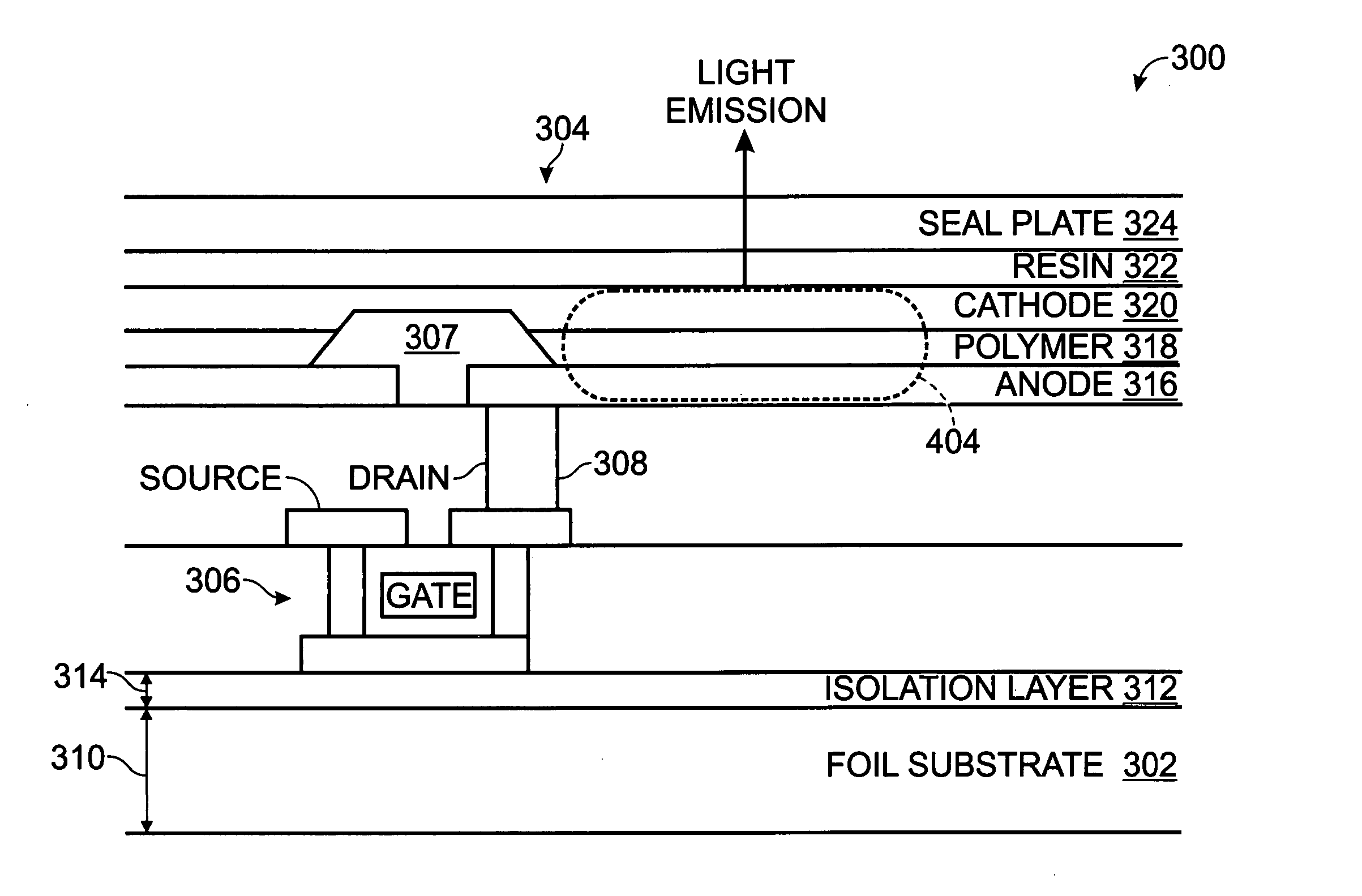
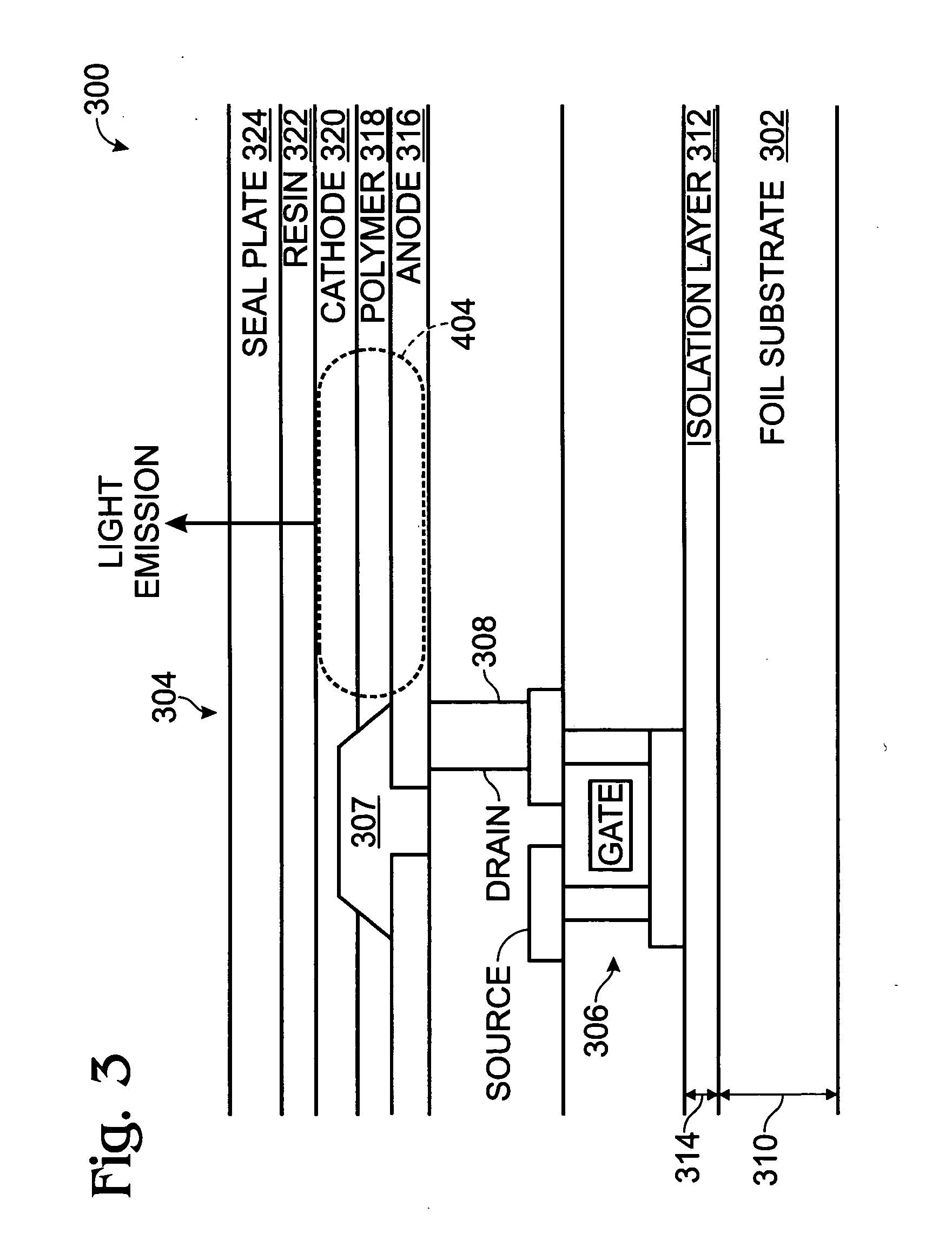
[0035]FIG. 3 is a partial cross-sectional view of the present invention flexible substrate, active matrix (AM), top emission organic light emitting diode (OLED) display. The display 300 comprises a metal foil substrate 302 and a plurality of pixels areas. For simplicity, a single pixel area 304 is shown. Each pixel area, including pixel area 304, includes at least one thin-film transistor (TFT) 306 overlying the substrate. The pixel area 304 is isolated with an isolation material 307.

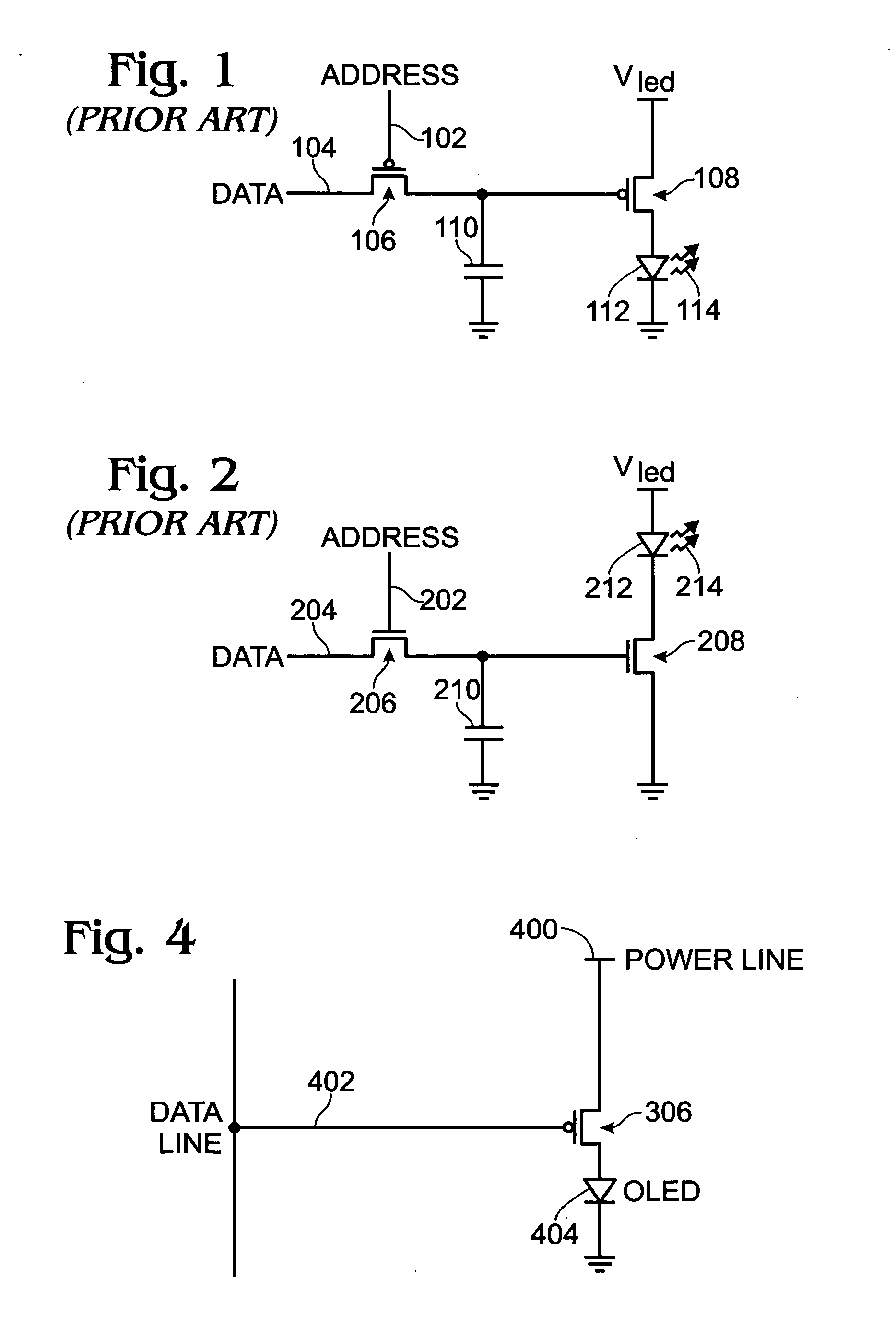
[0036]FIG. 4 is a schematic block diagram of the OLED display of FIG. 3, using a PNP transistor. As shown, first TFT 306 has a drain electrode connected to a power line 400, a gate electrode connected to a data line 402, and a source connected to the anode of an OLED 404. The cathode of the OLED 404 is connected to ground (or a voltage potential lower than the power line). As mentioned in the Background Section, PNP transistors are typically used when the cathode of the OLED 404 is grounded. The power ...


PUM


Abstract

A flexible metal foil substrate organic light emitting diode (OLED) display and a method for forming the same are provided. The method comprises: supplying a metal foil substrate such as titanium (Ti), Inconel alloy, or Kovar, having a thickness in the range of 10 to 500 microns; planarizing the metal foil substrate surface; depositing an electrical isolation layer having a thickness in the range of 0.5 to 2 microns overlying the planarized metal foil substrate surface; depositing amorphous silicon having a thickness in the range of 25 to 150 nanometers (nm) overlying the electrical insulation layer; from the amorphous silicon, forming polycrystalline silicon overlying the electrical insulation layer; forming thin-film transistors (TFTs) in the polycrystalline silicon; and, forming an electronic circuit using the TFTs, such as an OLED display.

Description

RELATED APPLICATIONS [0001] This application is a continuation-in-part of a pending patent application entitled, THIN-FILM TRANSISTORS FORMED ON A METAL FOIL SUBSTRATE, invented by Voutsas et al., Ser. No. 10 / 194,895, filed Jul. 11, 2002. [0002] This application is a Divisional of a pending patent application entitled, FLEXIBLE METAL FOIL SUBSTRATE DISPLAY AND METHOD FOR FORMING SAME, invented by Tolis Voutsas, Ser. No. 10 / 282,744, filed Oct. 28, 2002.BACKGROUND OF THE INVENTION [0003] 1. Field of the Invention [0004] This invention generally relates to organic light emitting diode (OLED) displays and, more particularly, to an OLED display fabricated on a thin metal foil substrate. [0005] 2. Description of the Related Art [0006] As noted in U.S. Pat. No. 6,392,617 (Robert Gleason), arrays of OLEDs are utilized to create two-dimensional flat panel displays. As compared to conventional light emitting diodes (LEDs), which are made of compound semiconductors, the low cost and ease of pa...

Claims


Application Information

Patent Timeline
IPC IPC(8): G02F1/1368G11C13/00H01L21/20H01L21/336H01L21/77H01L21/84H01L27/24H01L27/32H01L29/49H01L29/786H01L45/00H01L51/00
CPCG11C13/0007G11C2213/31H01L27/1214H01L27/3244H01L27/3262Y02E10/549H01L29/66757H01L29/78603H01L51/0097H01L2251/5315H01L2251/5338H01L29/4908H01L27/1262H01L27/1218Y02P70/50H10K59/1213H10K77/111H10K2102/3026H10K2102/311H10K59/12
Inventor VOUTSAS, APOSTOLOS T.
Owner SHARP LAB OF AMERICA INC
Why Eureka
Try Eureka